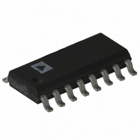
SSM2164S Analog Devices Inc, SSM2164S Datasheet - Page 7

SSM2164S
Manufacturer Part Number
SSM2164S
Description
IC AMP AUDIO QUAD CLASSAB 16SOIC
Manufacturer
Analog Devices Inc
Datasheet
1.SSM2164PZ.pdf
(12 pages)
Specifications of SSM2164S
Rohs Status
RoHS non-compliant
Amplifier Type
Audio
Number Of Circuits
4
Current - Input Bias
10nA
Current - Supply
6mA
Voltage - Supply, Single/dual (±)
8 V ~ 36 V, ±4 V ~ 18 V
Operating Temperature
-40°C ~ 85°C
Mounting Type
Surface Mount
Package / Case
16-SOIC (3.9mm Width)
Output Type
-
Current - Output / Channel
-
-3db Bandwidth
-
Slew Rate
-
Gain Bandwidth Product
-
Voltage - Input Offset
-
Available stocks
Company
Part Number
Manufacturer
Quantity
Price
Part Number:
SSM2164S
Manufacturer:
ADI/亚德诺
Quantity:
20 000
Company:
Part Number:
SSM2164SZ-REEL7
Manufacturer:
AD
Quantity:
1 000
REV. 0
–100
–20
–40
–60
–80
–45
–40
–35
–30
–25
–20
Figure 22. Gain Constant vs. Temperature
25
20
15
10
0
5
0
–50
10
1k
Figure 21. Supply Current vs. R
–ISY
Figure 20. PSRR vs. Frequency
V
T
V
+ISY
–25
S
A
S
= 15V
= +25 C
= 15V
100
10k
0
TEMPERATURE – C
FREQUENCY – Hz
+PSRR
1k
R
BIAS
25
–PSRR
–
10k
50
100k
CLASS A AND
CLASS AB
V
T
A
S
100K
= 15V
= +25 C
75
BIAS
100
1M
1M
–7–
APPLICATIONS INFORMATION
Circuit Description
The SSM2164 is a quad Voltage Controlled Amplifier (VCA)
with 120 dB of gain control range. Each VCA is a current-in,
current-out device with a separate –33 mV/dB voltage input
control port. The class of operation (either Class A or Class
AB) is set by a single external resistor allowing optimization of
the distortion versus noise tradeoff for a particular application.
The four independent VCAs in a single 16-pin package make
the SSM2164 ideal for applications where multiple volume
control elements are needed.
The simplified schematic in Figure 23 shows the basic structure
of one of the four VCAs in the device. The gain core is com-
prised of the matched differential pairs Q1-Q4 and the current
mirrors of Q5, Q6 and Q7, Q8. The current input pin, I
connected to the collectors of Q1 and Q7, and the difference in
current between these two transistors is equivalent to I
example, if 100 A is flowing into the input, Q1’s collector
current will be 100 A higher than Q7’s collector current.
Varying the control voltage V
one side of each differential pair to the other, resulting in either
gain or attenuation. For example, a positive voltage on V
steers more current through Q1 and Q4 and decreases the
current in Q2 and Q3. The current output pin, I
nected to the collector of Q3 and the current mirror (Q6) from
Q2. With less current flowing through these two transistors, less
current is available at the output. Thus, a positive V
the input and a negative V
unity gain for a control voltage of 0.0 V where the signal current
is divided equally between the gain core differential pairs.
The MODE pin allows the setting of the quiescent current in
the gain core of the VCA to trade off the SSM2164’s THD and
noise performance to an optimal level for a particular applica-
tion. Higher current through the core results in lower distortion
I
IN
Figure 23. Simplified Schematic (One Channel)
MODE
C
amplifies the input. The VCA has
C
Q5
, steers the signal current from
V+
V–
Q1
Q2
Q6
450
Q7
Q3
SSM2164
Q4
Q8
OUT
, is con-
500
C
4.5k
attenuates
IN
. For
IN
C
, is
I
V
OUT
C


