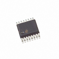
EL5304IU-T13 Intersil, EL5304IU-T13 Datasheet - Page 4

EL5304IU-T13
Manufacturer Part Number
EL5304IU-T13
Description
IC VFA SLEW TRPL 700MHZ 16-QSOP
Manufacturer
Intersil
Datasheet
1.EL5104ISZ.pdf
(17 pages)
Specifications of EL5304IU-T13
Amplifier Type
Voltage Feedback
Number Of Circuits
3
Slew Rate
3000 V/µs
-3db Bandwidth
700MHz
Current - Input Bias
8µA
Voltage - Input Offset
5000µV
Current - Supply
9.5mA
Current - Output / Channel
160mA
Voltage - Supply, Single/dual (±)
4 V ~ 13.2 V, ±2 V ~ 6.6 V
Operating Temperature
-40°C ~ 85°C
Mounting Type
Surface Mount
Package / Case
16-QSOP
Lead Free Status / RoHS Status
Contains lead / RoHS non-compliant
Output Type
-
Gain Bandwidth Product
-
Absolute Maximum Ratings
Supply Voltage between V
Input Voltage . . . . . . . . . . . . . . . . . . . . . . . . . . . . . . . . . . . . . . . .±V
Differential Input Voltage . . . . . . . . . . . . . . . . . . . . . . . . . . . . . . .±4V
Maximum Output Current. . . . . . . . . . . . . . . . . . . . . . . . . . . . . 80mA
V
CAUTION: Stresses above those listed in “Absolute Maximum Ratings” may cause permanent damage to the device. This is a stress only rating and operation of the
device at these or any other conditions above those indicated in the operational sections of this specification is not implied.
IMPORTANT NOTE: All parameters having Min/Max specifications are guaranteed. Typical values are for information purposes only. Unless otherwise noted, all tests
are at the specified temperature and are pulsed tests, therefore: T
DC Electrical Specifications
V
TCV
IB
I
TCI
PSRR
CMRR
CMIR
R
C
I
I
PSOR
AVOL
V
V
I
V
V
S
OS
S,ON
S,OFF
OUT
PARAMETER
OS
IN
IN
OP
ON
IH-EN
IL-EN
+ to V
OS
OS
S
- Maximum Slew Rate . . . . . . . . . . . . . . . . . . . . . . . 1V/µs
Offset Voltage
Offset Voltage Temperature Coefficient
Input Bias Current
Input Offset Current
Input Bias Current Temperature
Coefficient
Power Supply Rejection Ratio
Common Mode Rejection Ratio
Common Mode Input Range
Input Resistance
Input Capacitance
Supply Current - Enabled
Supply Current - Shut Down
Power Supply Operating Range
Open Loop Gain
Positive Output Voltage Swing
Negative Output Voltage Swing
Output Current
ENABLE Pin Voltage for Power Up
ENABLE Pin Voltage for Shut Down
S
+ and GND. . . . . . . . . . . . . . . . . . 13.2V
DESCRIPTION
4
(T
EL5104, EL5105, EL5204, EL5205, EL5304
A
V
Specified.
= +25°C)
S
= ±5V, GND = 0V, T
J
= T
EL5104, EL5105, EL5204, EL5205
EL5304
Measured from T
V
V
Measured from T
V
Guaranteed by CMRR test
Common mode
SO package
Per amplifier
V
V
R
R
R
R
R
C
IN
IN
CM
S
S
L
L
L
L
L
= T
A
+, per amplifier
-, per amplifier
= 1kΩ to GND
= 150Ω to GND
= 150Ω to 0V
= 150Ω to 0V
= 10Ω to 0V
= 0V
= 0V
= +25°C, V
S
A
from -3V to +3V
CONDITIONS
CM
Thermal Information
Storage Temperature Range . . . . . . . . . . . . . . . . . .-65°C to +150°C
Ambient Operating Temperature Range . . . . . . . . . .-40°C to +85°C
Operating Junction Temperature . . . . . . . . . . . . . . . . . . . . . . +150°C
Pb-free reflow profile . . . . . . . . . . . . . . . . . . . . . . . . . .see link below
MIN
MIN
http://www.intersil.com/pbfree/Pb-FreeReflow.asp
= 0V, V
to T
to T
MAX
MAX
OUT
= 0V, V
ENABLE
= GND or OPEN, Unless Otherwise
(V
(V
MIN
±90
-10
-18
-25
8.5
3.6
+1
60
56
50
55
-3
-5
-1
4
S
S
+)
+)
±160
TYP
120
-3.8
9.5
3.8
10
50
70
62
17
65
60
3
5
8
4
1
0
(V
MAX
13.2
V
+25
-3.6
10
18
30
15
+3
11
-1
-3
S
S
+)
+
May 3, 2007
µV/°C
nA/°C
FN7332.6
UNIT
mV
mV
mA
mA
kΩ
µA
µA
dB
dB
pF
µA
µA
dB
dB
V
V
V
V
V
V


