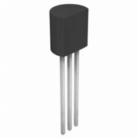
MCP121-450E/TO Microchip Technology, MCP121-450E/TO Datasheet - Page 12

MCP121-450E/TO
Manufacturer Part Number
MCP121-450E/TO
Description
IC SUPERVISOR 4.38V LOW TO-92
Manufacturer
Microchip Technology
Type
Simple Reset/Power-On Resetr
Datasheet
1.MCP131T-270ETT.pdf
(28 pages)
Specifications of MCP121-450E/TO
Number Of Voltages Monitored
1
Output
Open Drain or Open Collector
Reset
Active Low
Reset Timeout
80 ms Minimum
Voltage - Threshold
4.38V
Operating Temperature
-40°C ~ 125°C
Mounting Type
Through Hole
Package / Case
TO-92-3 (Standard Body), TO-226
Threshold Voltage
4.38V
No. Of Supervisors / Monitors
1
Supply Voltage Range
1V To 5.5V
Reset Type
Active-Low
Supply Current
20µA
Delay Time
120ms
Digital Ic Case Style
TO-92
Lead Free Status / RoHS Status
Lead free / RoHS Compliant
MCP102/103/121/131
4.0
For many of today’s microcontroller applications, care
must be taken to prevent low-power conditions that can
cause many different system problems. The most
common causes are brown-out conditions, where the
system supply drops below the operating level momen-
tarily. The second most common cause is when a
slowly
microcontroller to begin executing instructions without
sufficient voltage to sustain volitile memory (RAM), thus
producing indeterminate results. Figure 4-1 shows a
typical application circuit.
The MCP102/103/121/131 are voltage supervisor
devices designed to keep a microcontroller in reset
until the system voltage has reached and stabilized at
the proper level for reliable system operation. These
devices also operate as protection from brown-out
conditions.
FIGURE 4-1:
FIGURE 4-2:
DS21906B-page 12
0.1
µF
V
Note 1: Resistor R
DD
APPLICATION INFORMATION
decaying
MCP1XX
MCP121 due to the open-drain output.
Resistor R
the MCP131 due to the internal pull-up
resistor. The MCP102 and MCP103 do
not require the external pull-up resistor.
V
RST
V
V
DD
SS
DD
RST
V
power
Typical Application Circuit.
TRIPMAX
RST
PU
PU
V
TRIPMIN
t
RPD
may be required with the
may not be required with
Operation as Determined by the V
supply
R
PU
1V
Microcontroller
MCLR
(Reset input)
(Active-low)
PICmicro
causes
< 1V is outside the
V
device specifications
V
SS
DD
®
the
V
TRIPAC
+ V
4.1
The RST output pin operation determines how the
device can be used and indicates when the system
should be forced into reset. To accomplish this, an
internal voltage reference is used to set the voltage trip
point (V
trip point.
When the falling edge of V
threshold, the reset power-down timer (T
When this delay timer times out, the RST pin is forced
low.
When the rising-edge of V
threshold, the reset power-up timer (T
When this delay timer times out, the RST pin is forced
high, T
current.
The actual voltage trip point (V
the minimum trip point (V
trip point (V
and the delay timer (T
that would occur on the RST pin when the device V
is at the trip point.
Figure 4-2 shows the waveform of the RST pin as deter-
mined by the V
state of the RST pin. The V
V
will not be driven high until V
V
minimal delay time (T
low.
TABLE 4-1:
Device
MCP102
MCP103
MCP121
MCP131
HYSAC
DD
DD
TRIP
Note 1: Requires External Pull-up resistor
voltages. When the V
has crossed the voltage trip point, there is also a
TRIP
and V
RPU
2: Has Internal Pull-up resistor
RST Operation
V
). Additionally, there is a hysteresis on this
TRIPMAX
State of RST Pin when:
DD
is active and there is additional system
V
t
HYS
TRIPAC
RPU
DD
< V
L
L
L
L
t
RST PIN STATES
RPD
.
TRIP
voltage, while Table 4-1 shows the
). The hysteresis on this trip point
RPD
RPU
© 2005 Microchip Technology Inc.
V
V
) before the RST pin is driven
TRIP
DD
DD
TRIP
TRIPMIN
) are to remove any “jitter”
DD
DD
H
H
DD
voltage is rising, the RST
>
is at V
specification is for falling
TRIPAC
H
H
+ V
(1)
(2)
V
crosses this voltage
crosses this voltage
TRIPAC
) and the maximum
t
HYS
RPU
TRIP
) will be between
Ouput Driver
Push-pull
Push-pull
Open-drain
Open-drain
+ V
RPU
RPD
HYS
) starts.
) starts.
. Once
(1)
(2)
DD


