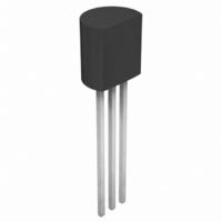
MCP121-450E/TO Microchip Technology, MCP121-450E/TO Datasheet - Page 13

MCP121-450E/TO
Manufacturer Part Number
MCP121-450E/TO
Description
IC SUPERVISOR 4.38V LOW TO-92
Manufacturer
Microchip Technology
Type
Simple Reset/Power-On Resetr
Datasheet
1.MCP131T-270ETT.pdf
(28 pages)
Specifications of MCP121-450E/TO
Number Of Voltages Monitored
1
Output
Open Drain or Open Collector
Reset
Active Low
Reset Timeout
80 ms Minimum
Voltage - Threshold
4.38V
Operating Temperature
-40°C ~ 125°C
Mounting Type
Through Hole
Package / Case
TO-92-3 (Standard Body), TO-226
Threshold Voltage
4.38V
No. Of Supervisors / Monitors
1
Supply Voltage Range
1V To 5.5V
Reset Type
Active-Low
Supply Current
20µA
Delay Time
120ms
Digital Ic Case Style
TO-92
Lead Free Status / RoHS Status
Lead free / RoHS Compliant
4.2
The minimum pulse width (time) required to cause a
reset may be an important criteria in the implementa-
tion of a Power-on Reset (POR) circuit. This time is
referred to as transient duration, defined as the amount
of time needed for these supervisory devices to
respond to a drop in V
dependant on the magnitude of V
speaking, the transient duration decreases with
increases in V
Figure 4-3 shows a typical transient duration vs. reset
comparator
MCP102/103/121/131 will not generate a reset pulse. It
shows that the farther below the trip point the transient
pulse goes, the duration of the pulse required to cause
a reset gets shorter. Figure 2-32 shows the transient
response characteristics for the MCP102/103/121/131.
A 0.1 µF bypass capacitor, mounted as close as
possible to the V
immunity (refer to Figure 4-1).
FIGURE 4-3:
Transient Duration Waveform.
© 2005 Microchip Technology Inc.
5V
0V
Negative Going V
TRIP
overdrive,
DD
t
– V
TRANS
Time (µs)
pin, provides additional transient
DD
DD
Example of Typical
. The transient duration time is
.
V
TRIP(MIN)
DD
for
TRIP
Transients
– V
- V
which
DD
DD
V
V
. Generally
TRIP(MAX)
TRIP(MIN)
the
4.3
Figure 4-4 illustrates the device current states. While
the system is powering down, the device has a low
current. This current is dependent on the device V
and trip point. When the device V
voltage trip point (V
timer consumes additional current until the RST pin is
driven (or released) high. This time is known as the
Reset Power-up Time (t
t
FIGURE 4-4:
Waveform.
4.3.1
The Reset Power-up timer time-out period (t
determines how long the device remains in the reset
condition. This is affected by both V
Typical responses for different V
temperatures are shown in Figures 2-26, 2-27 and 2-28.
MCP102/103/121/131
RPU
RST
V
DD
is active (device consuming additional current).
V
TRIP
See Figures 2-1,
Reset Power-up Timer (t
2-2 and 2-3
EFFECT OF TEMPERATURE ON
RESET POWER-UP TIMER (T
Reset Power-up
Timer Inactive
TRIP
Reset Power-up Timer
), an internal timer starts. This
RPU
See Figures 2-4,
2-5 and 2-6
). Figure 4-4 shows when
t
DD
RPU
DD
DS21906B-page 13
See Figures 2-1,
rises through the
and temperature.
DD
2-2 and 2-3
RPU
Reset
Power-up
Timer
Inactive
values and
)
RPU
)
RPU
DD
)


