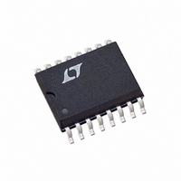
LTC695CSW-3.3#PBF Linear Technology, LTC695CSW-3.3#PBF Datasheet - Page 7

LTC695CSW-3.3#PBF
Manufacturer Part Number
LTC695CSW-3.3#PBF
Description
IC MPU SUPRVSRY CIRC 3.3V 16SOIC
Manufacturer
Linear Technology
Type
Simple Reset/Power-On Resetr
Datasheet
1.LTC694CS8-3.3PBF.pdf
(20 pages)
Specifications of LTC695CSW-3.3#PBF
Number Of Voltages Monitored
1
Output
Open Drain or Open Collector
Reset
Active High/Active Low
Reset Timeout
140 ms Minimum
Voltage - Threshold
2.9V
Operating Temperature
0°C ~ 70°C
Mounting Type
Surface Mount
Package / Case
16-SOIC (0.300", 7.5mm Width)
Lead Free Status / RoHS Status
Lead free / RoHS Compliant
Available stocks
Company
Part Number
Manufacturer
Quantity
Price
PIN FUNCTIONS
BATT ON: Battery On Logic Output from Comparator C2.
BATT ON goes low when V
V
base drive for an external PNP transistor to increase the
output current above the 50mA rating of V
goes high when V
CE IN: Logic Input to the Chip
can be derived from microprocessor’s address line and/or
decoder output. See the Applications Information section
and Figure 5 for additional information.
CE OUT: Logic Output on the Chip
When V
a buffered replica of CE IN. When V
voltage threshold CE OUT is forced high (see Figure 5).
GND: Ground Pin.
LOW
indicates a low line condition at the V
falls below the reset voltage threshold (2.90V typically),
LOW
voltage threshold, LOW
LOW
Table 1).
OSC IN: Oscillator Input. OSC IN can be driven by an
external clock signal or an external capacitor can be con-
nected between OSC IN and GND when OSC SEL is forced
low. In this configuration the nominal reset active time and
watchdog timeout period are determined by the number
of clocks or set by the formula (see the Applications In-
formation section). When OSC SEL is high or floating, the
internal oscillator is enabled and the reset active time is
fixed at 200ms typical for the LTC695-3.3. OSC IN selects
between the 1.6 seconds and 100ms typical watchdog
timeout periods. In both cases, the timeout period im-
mediately after a reset is 1.6 seconds typical.
OSC SEL: Oscillator Selection Input. When OSC SEL is
high or floating, the internal oscillator sets the reset active
time and watchdog timeout period. Forcing OSC SEL low,
allows OSC IN to be driven from an external clock signal
or an external capacitor can be connected between OSC
IN and GND.
CC
. The output typically sinks 25mA and can provide
_
_
_
LINE: Logic Output from Comparator C1. LOW
LINE goes low. As soon as V
LINE goes low when V
CC
is above the reset voltage threshold, CE OUT is
OUT
is internally switched to V
_
LINE returns high (see Figure 1).
OUT
_
CC
Enable Gating Circuit. CE IN
is internally connected to
drops below V
CC
_
Enable Gating Circuit.
CC
rises above the reset
CC
is below the reset
input. When V
OUT
. BATT ON
BATT
BATT
_
LINE
.
(see
CC
PFI: Power Failure Input. PFI is the noninverting input
to the power-fail comparator, C3. The inverting input is
internally connected to a 1.3V reference. The power failure
output remains high when PFI is above 1.3V and goes
low when PFI is below 1.3V. Connect PFI to GND or V
when C3 is not used.
PFO: Power Failure Output from C3. PFO remains high
when PFI is above 1.3V and goes low when PFI is below
1.3V. When V
PFO is forced low.
RESET: Active High Logic Output. It is the inverse of
RESET.
RESET: Logic Output for μP Reset Control. Whenever V
falls below either the reset voltage threshold (2.90V, typi-
cally) or V
to 3.3V, the reset pulse generator forces RESET to remain
active low for a minimum of 140ms. When the watchdog
timer is enabled but not serviced prior to a preset timeout
period, the reset pulse generator also forces RESET to ac-
tive low for a minimum of 140ms for every preset timeout
period (see Figure 11). The reset active time is adjustable
on the LTC695-3.3. An external push-button reset can be
used in connection with the RESET output. See Push-But-
ton Reset in the Applications Information section.
V
auxiliary power connected to V
through PMOS switch, M2. If back-up battery or auxiliary
power is not used, V
V
with a 0.1μF capacitor.
V
a capacitor of 0.1μF or greater. During normal operation,
V
switch, M1, which can deliver up to 50mA and has a typical
on resistance of 5Ω. When V
is internally switched to V
used, connect V
BATT
CC
OUT
OUT
: 3.3V Supply Input. The V
: Voltage Output for Backed Up Memory. Bypass with
: Back-Up Battery Input. When V
obtains power from V
LTC694-3.3/LTC695-3.3
BATT
CC
, RESET goes active low. After V
is lower than V
OUT
to V
BATT
CC
should be connected to GND.
BATT
.
CC
CC
. If V
CC
BATT
through an NMOS power
BATT
is lower than V
pin should be bypassed
OUT
, C3 is shut down and
, is delivered to V
CC
and V
falls below V
BATT
CC
BATT
returns
are not
, V
69453fb
BATT
7
OUT
OUT
OUT
CC
,


