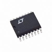
LTC695CSW-3.3#PBF Linear Technology, LTC695CSW-3.3#PBF Datasheet - Page 9

LTC695CSW-3.3#PBF
Manufacturer Part Number
LTC695CSW-3.3#PBF
Description
IC MPU SUPRVSRY CIRC 3.3V 16SOIC
Manufacturer
Linear Technology
Type
Simple Reset/Power-On Resetr
Datasheet
1.LTC694CS8-3.3PBF.pdf
(20 pages)
Specifications of LTC695CSW-3.3#PBF
Number Of Voltages Monitored
1
Output
Open Drain or Open Collector
Reset
Active High/Active Low
Reset Timeout
140 ms Minimum
Voltage - Threshold
2.9V
Operating Temperature
0°C ~ 70°C
Mounting Type
Surface Mount
Package / Case
16-SOIC (0.300", 7.5mm Width)
Lead Free Status / RoHS Status
Lead free / RoHS Compliant
Available stocks
Company
Part Number
Manufacturer
Quantity
Price
APPLICATIONS INFORMATION
Microprocessor Reset
The LTC694-3.3/LTC695-3.3 use a bandgap voltage refer-
ence and a precision voltage comparator C1 to monitor the
3.3V supply input on V
V
put is forced to active low state. The reset voltage threshold
accounts for a 10% variation on V
becomes active low when V
cal). On power-up, the RESET signal is held active low for a
minimum of 140ms after reset voltage threshold is reached
to allow the power supply and microprocessor to stabilize.
The reset active time is adjustable on the LTC695-3.3.
On power-down, the RESET signal remains active low
even with V
microprocessor in stable shutdown condition. Figure 1
shows the timing diagram of the RESET signal.
The precision voltage comparator, C1, typically has 40mV
of hysteresis which ensures that glitches at V
not activate the RESET output. Response time is typically
10ms. To help prevent mistriggering due to transient loads,
the V
with the leads trimmed as short as possible.
The LTC695-3.3 has two additional outputs: RESET and
LOW
of RESET. LOW
comparator C1. When V
threshold, LOW
soon as V
CC
falls below the reset voltage threshold, the RESET out-
_
CC
LINE. RESET is an active high output and is the inverse
pin should be bypassed with a 0.1μF capacitor
CC
CC
rises above the reset voltage threshold.
as low as 1V. This capability helps hold the
_
LOW LINE
_
LINE is the output of the precision voltage
LINE goes low. LOW
RESET
V
CC
CC
CC
(see the Block Diagram). When
CC
falls below the reset voltage
V2
falls below 3.0V (2.9V typi-
CC
t
1
, so the RESET output
_
LINE returns high as
Figure 1. Reset Active Time
CC
pin do
V1
V2
Battery Switchover
The battery switchover circuit compares V
input, and connects V
V
comparator, C2, connects V
pumped NMOS power switch, M1. When V
above V
switch, M2. C2 has typically 20mV of hysteresis to prevent
spurious switching when V
The response time of C2 is approximately 20μs.
During normal operation, the LTC694-3.3/LTC695-3.3 use
a charge-pumped NMOS power switch to achieve low
dropout and low supply current. This power switch can
deliver up to 50mA to V
resistance of 5Ω. The V
a capacitor of 0.1μF or greater to ensure stability. Use of
a larger bypass capacitor is advantageous for supplying
current to heavy transient loads.
When operating currents larger than 50mA are required
from V
ferential) is desired, the LTC695-3.3 should be used. This
product provides BATT ON output to drive the base of
an external PNP transistor (Figure 2). If higher currents
are needed with the LTC694-3.3, a high current Schottky
diode can be connected from the V
to supply the extra current.
CC
rises to 70mV above V
V1 = RESET VOLTAGE THRESHOLD
V2 = RESET VOLTAGE THRESHOLD +
t
1
= RESET ACTIVE TIME
OUT
BATT
t
RESET THRESHOLD HYSTERESIS
1
LTC694-3.3/LTC695-3.3
, or a lower dropout (V
, C2 connects V
OUT
OUT
OUT
CC
to whichever is higher. When
OUT
from V
OUT
pin should be bypassed with
remains nearly equal to V
BATT
to V
to V
, the battery switchover
V1
CC
CC
CC
BATT
694/5-3.3 F01
CC
and has a typical on
– V
pin to the V
through a charge
through a PMOS
OUT
CC
CC
falls to 50mV
to the V
voltage dif-
OUT
69453fb
BATT
BATT
9
pin
.


