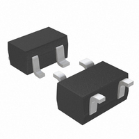
XC6120N182NR-G Torex Semiconductor Ltd, XC6120N182NR-G Datasheet - Page 6

XC6120N182NR-G
Manufacturer Part Number
XC6120N182NR-G
Description
IC SUPERVISOR 1.8V SSOT24-4
Manufacturer
Torex Semiconductor Ltd
Type
Simple Reset/Power-On Resetr
Datasheet
1.XC6120C182NR-G.pdf
(13 pages)
Specifications of XC6120N182NR-G
Number Of Voltages Monitored
1
Output
Open Drain or Open Collector
Voltage - Threshold
1.8V
Operating Temperature
-40°C ~ 85°C
Mounting Type
Surface Mount
Package / Case
SSOT-24, SuperSOT-24 (SC-82)
Lead Free Status / RoHS Status
Lead free / RoHS Compliant
Reset
-
Reset Timeout
-
Other names
893-1021-2
6/13
■OPERATIONAL EXPLANATION
●Typical Application Circuit
The following explains the operation of the typical application circuit along number symbols shown in the timing chart.
① When input voltage (V
② When input voltage (V
③ When input voltage (V
④ When input voltage (V
⑤ When the input voltage (V
⑥ The difference between V
XC6120
●Timing Charge
V
IN
(A condition of high impedance exists with N-ch open drain output configurations.)
(V
unstable. If In this condition, V
the typical application circuit.)
(V
(V
SS
DR
IN
). (A condition of high impedance exists with N-ch open drain output configurations.)
) level.
), output keeps the ground voltage level (V
Input Voltage
Note: For explaining in a simplified case, an operation time of the circuit is not counted.
Voltage
Output
Series
(V
(V
OUT
V
V
SS
IN
IN
)
)
IN
IN
V
IN
IN
) is higher than detect voltage (V
OUT
) falls below detect voltage (V
) rises above the minimum operating voltage (V
) falls to a level below that of the minimum operating voltage (V
DR
IN
) rises above the release voltage (V
and V
IN
①
R
(Unused for the CMOS output products)
will equal the pulled-up output (should output be pulled-up.) (Input voltage, V
DF
PULL
V
represents the hysteresis width.
OUT
②
SS
).
③
DF
DF
), output voltage (V
), output voltage (V
④
DR
), output voltage (V
⑥
⑤
MIN
) level until it achieves a release voltage
OUT
OUT
) will be equal to the ground voltage
) will be equal to input voltage (V
Release Voltage (V
Minimum Operating Voltage (V
Detect Voltage (V
Ground Voltage (V
Ground Voltage (V
OUT
will be equal to input voltage
MIN
), output will become
DF
SS
SS
DR
)
)
)
)
IN
MIN
, in
IN
).
)


