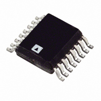
ADM2914-2ARQZ Analog Devices Inc, ADM2914-2ARQZ Datasheet - Page 11

ADM2914-2ARQZ
Manufacturer Part Number
ADM2914-2ARQZ
Description
IC MONITOR 4CH UV/OV 16-QSOP
Manufacturer
Analog Devices Inc
Type
Multi-Voltage Supervisorr
Datasheet
1.EVAL-ADM2914EBZ.pdf
(16 pages)
Specifications of ADM2914-2ARQZ
Number Of Voltages Monitored
4
Output
Open Drain or Open Collector
Reset
Active Low
Reset Timeout
Adjustable/Selectable
Voltage - Threshold
Adjustable/Selectable
Operating Temperature
-40°C ~ 125°C
Mounting Type
Surface Mount
Package / Case
16-QSOP
Threshold Voltage
1V
No. Of Supervisors / Monitors
4
Supply Voltage Range
2.3V To 6.9V
Reset Type
Active-Low / Open-Drain
Supply Current
100µA
Delay Time
8.5ms
Lead Free Status / RoHS Status
Lead free / RoHS Compliant
Next, consider a −12 V input, which is specified with a ±20%
input. The threshold accuracy required by the supply is chosen
to be within ±5% of the −12 V rail. Therefore, the overvoltage
threshold is set to −13.5 V, and the undervoltage threshold is
−10.5 V. The negative voltage scheme configuration requires
that the 1 V reference voltage be accounted for in Equation 1 to
Equation 3. The 1 V reference voltage is subtracted from V
V
Equation 1 becomes
Insert the value of R
To calculate R
POWER-UP AND POWER-DOWN
On power-up, when V
is asserted, and the OV output pulls up to V
tage on the V
assert UV low and OV high. When V
the VHx and VLx inputs take control. When V
the VHx inputs are valid, an internal timer begins. Subsequent
to an adjustable time delay, UV weakly pulls high.
UV/OV TIMING CHARACTERISTICS
UV is an active low output. It is asserted when any of the four
monitored voltages is below its associated threshold. When the
voltage on the V
UV low for an adjustable period, t
the monitoring rails rises above their thresholds. This allows
time for all monitored power supplies to stabilize after power-
up. Similarly, any monitored voltage that falls below its threshold
initiates a timer reset, and the timer starts again when all the
monitoring rails rise above their thresholds.
The UV and OV outputs are held asserted after all faults have
cleared for an adjustable timeout period, determined by the
value of the external capacitor attached to the TIMER pin.
TIMER CAPACITOR SELECTION
The UV and OV timeout period on the ADM2914 is programma-
ble via the external timer capacitor, C
TIMER pin and ground. The timeout period, t
using the following equation:
UV
, and V
C
R
R
R
Y
TIMER
Z
X
=
=
=
OV
(
(
(
5
−
−
−
=
, and the absolute value of the result is taken.
CC
×
13
10
12
0 (
X
0 (
(
, insert the value of R
10
t
pin reaches 1 V, the ADM2914 is guaranteed to
) 5 .
UOTO
5 .
5 .
) 5 .
CC
−
−
−
−
1
(
6
pin is above 2 V, an internal timer holds
(
−
1
1
−
Z
)
)(
12
)
)
12
−
into Equation 2.
(
(
CC
115
5
5
(
×
−
×
89
−
reaches 1 V, the active low UV output
10
10
1
)(
1
8 .
)
10
)
−
−
kΩ
6
6
9 −
)
)
−
) (
)
≈
−
89
F/sec
UOTO
89
23
8 .
CC
Z
8 .
TIMER
and R
kΩ
4 .
exceeds 1.9 V (minimum),
, after the voltage on all
kΩ
kΩ
≈
, placed between the
23
Y
)
CC
≈
into Equation 3.
. When the vol-
4 .
. 2
UOTO
CC
kΩ
49
and each of
, is calculated
MΩ
M
,
Rev. B | Page 11 of 16
Refer to Figure 15 in the Typical Performance Characteristics
section, which illustrates the delay time as a function of the
timer capacitor value. A minimum capacitor value of 10 pF is
required. The chosen timer capacitor must have a leakage current
that is less than the 1.3 μA TIMER pin charging current. To
bypass the timeout period, connect the TIMER pin to V
WHEN AN INPUT IS CONFIGURED TO MONITOR A NEGATIVE VOLTAGE,
VLx WILL TRIGGER AN UNDERVOLTAGE CONDITION.
WHEN AN INPUT IS CONFIGURED TO MONITOR A NEGATIVE VOLTAGE,
VHx WILL TRIGGER AN OVERVOLTAGE CONDITION.
VHx
VHx
UV
UV
VLx
OV
Figure 21. VHx Positive Voltage Monitoring Timing Diagram
VLx
Figure 22. VLx Positive Voltage Monitoring Timing Diagram
OV
t
t
V
V
UOD
UOD
t
UOD
UOT
UOT
V
VHx MONITOR TIMING (TIMER PIN TIED TO V
UOT
V
t
VLx MONITOR TIMING (TIMER PIN TIED TO V
UOD
UOT
1V
1V
1V
1V
VHx MONITOR TIMING
VLx MONITOR TIMING
t
UOTO
t
t
UOTO
UOD
t
UOD
CC
CC
)
ADM2914
)
CC
.


