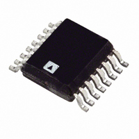
ADM2914-2ARQZ Analog Devices Inc, ADM2914-2ARQZ Datasheet - Page 9

ADM2914-2ARQZ
Manufacturer Part Number
ADM2914-2ARQZ
Description
IC MONITOR 4CH UV/OV 16-QSOP
Manufacturer
Analog Devices Inc
Type
Multi-Voltage Supervisorr
Datasheet
1.EVAL-ADM2914EBZ.pdf
(16 pages)
Specifications of ADM2914-2ARQZ
Number Of Voltages Monitored
4
Output
Open Drain or Open Collector
Reset
Active Low
Reset Timeout
Adjustable/Selectable
Voltage - Threshold
Adjustable/Selectable
Operating Temperature
-40°C ~ 125°C
Mounting Type
Surface Mount
Package / Case
16-QSOP
Threshold Voltage
1V
No. Of Supervisors / Monitors
4
Supply Voltage Range
2.3V To 6.9V
Reset Type
Active-Low / Open-Drain
Supply Current
100µA
Delay Time
8.5ms
Lead Free Status / RoHS Status
Lead free / RoHS Compliant
MONITORING PIN CONNECTIONS
Positive Voltage Monitoring Scheme
When monitoring a positive supply, the desired nominal
operating voltage for monitoring is denoted by V
nominal current through the resistor divider, V
overvoltage trip point, and V
Figure 17 illustrates the positive voltage monitoring input connec-
tion. Three external resistors, R
voltage for monitoring, V
low-side voltage, V
corresponding VHx pin, and the low-side voltage is connected
to the corresponding VLx pin.
To trigger an overvoltage condition, the low-side voltage (in this
case, V
low-side voltage, V
Also,
Therefore, R
overvoltage monitor, is calculated using the following equation:
Figure 17. Positive Undervoltage/Overvoltage Monitoring Configuration
V
R
R
PL
X
Z
PL
) must exceed the 0.5 V threshold on the VLx pin. The
+
=
=
R
(
V
0 (
V
Y
Z
OV
, which sets the desired trip point for the
OV
) 5 .
+
⎛
⎜
⎜
⎝
R
( )
) ( )
V
V
V
R
R
R
I
PH
R
Z
PL
M
X
Y
Z
M
PL
PL
X
V
=
M
. The high-side voltage is connected to the
, is given by the following equation:
+
V
I
R
R
M
M
Y
Z
M
VHx
VLx
+
, into high-side voltage, V
R
UV
Z
X
is the undervoltage trip point.
⎞
⎟
⎟
⎠
, R
=
ADM2914
Y
0
, and R
0.5V
5 .
V
UVx
OVx
Z
, divide the positive
OV
M
is the
, I
M
PH
is the
, and
Rev. B | Page 9 of 16
(1)
To trigger the undervoltage condition, the high-side voltage,
V
high-side voltage, V
Because R
When R
equation:
If V
Negative Voltage Monitoring Scheme
Figure 18 shows the circuit configuration for negative supply
voltage monitoring. To monitor the negative voltage, a 1 V
reference voltage is required to connect to the end node of the
voltage divider circuit. This reference voltage is generated
internally and is output through the REF pin.
The equations described in the Positive Voltage Monitoring
Scheme section need some minor modifications for use with
negative voltage monitoring. The 1 V reference voltage is added
to the overall voltage drop; it must therefore be subtracted from
V
To monitor a negative voltage level, the resistor divider circuit
divides the voltage differential level between the 1 V reference
voltage and the negative supply voltage into high-side voltage,
V
monitoring scheme, the high-side voltage, V
the corresponding VH
connected to the corresponding VL
Monitoring Example section for more information.
Figure 18. Negative Undervoltage/Overvoltage Monitoring Configuration
PH
M
NH
, V
, must exceed the 0.5 V threshold on the VHx pin. The
M
, and low-side voltage, V
V
, I
R
R
UV
PH
Y
X
M
, and V
Y
, V
=
=
and R
=
Z
(
( )
0 (
OV
( )
is already known, R
V
V
V
I
UV
UV
) 5 .
, or V
M
M
OV
Z
( )
⎛
⎜
⎜
⎝
) ( )
V
V
−
V
are known, R
R
I
R
NH
R
R
NL
before using each in the previous equations.
M
M
R
Z
Y
X
UV
X
V
PH
R
Z
M
+
, is given by the following equation:
changes, each step must be recalculated.
Y
−
−
X
R
+
R
R
pin, and the low-side voltage, V
Y
Z
Y
R
VHx
VLx
+
REF
Z
NL
R
Z
X
. Similar to the positive voltage
Y
is calculated using the following
⎞
⎟
⎟
⎠
can be expressed as follows:
=
ADM2914
X
0
0.5V
5 .
pin. Refer to the Voltage
V
OVx
UVx
NH
, is connected to
ADM2914
NL
, is
(2)
(3)


