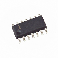
X5645S14 Intersil, X5645S14 Datasheet - Page 2

X5645S14
Manufacturer Part Number
X5645S14
Description
IC CPU SUPRV 64K EE RST HI SO14
Manufacturer
Intersil
Type
Simple Reset/Power-On Resetr
Datasheet
1.X5643P.pdf
(19 pages)
Specifications of X5645S14
Number Of Voltages Monitored
1
Output
Open Drain or Open Collector
Reset
Active High
Reset Timeout
100 ms Minimum
Voltage - Threshold
4.38V
Operating Temperature
0°C ~ 70°C
Mounting Type
Surface Mount
Package / Case
14-SOIC (3.9mm Width), 14-SOL
Lead Free Status / RoHS Status
Contains lead / RoHS non-compliant
PIN CONFIGURATION
PDIP
Pin
CS/WDI
1
2
5
6
3
4
8
7
V
SO
WP
SS
12 & 13
1, 7, 8,
SOIC
2 & 3
Pin
10
11
14
4
9
5
6
1
2
3
4
8-Lead PDIP
X5643/45
15-17, 20
TSSOP
1, 4-6,
9-12,
Pin
13
14
19
18
2
3
7
8
2
8
7
6
5
CS/WDI
RESET/
RESET
Name
SCK
V
V
WP
SO
NC
SI
SS
CC
V
RESET/RESET
SCK
SI
CC
Chip Select Input. CS HIGH, deselects the device and the SO output pin is at
a high impedance state. Unless a nonvolatile write cycle is underway, the de-
vice will be in the standby power mode. CS LOW enables the device, placing it
in the active power mode. Prior to the start of any operation after power-up, a
HIGH to LOW transition on CS is required.
Watchdog Input. A HIGH to LOW transition on the WDI pin restarts the watchdog
timer. The absence of a HIGH to LOW transition within the watchdog time out
period results in RESET/RESET going active.
Serial Output. SO is a push/pull serial data output pin. A read cycle shifts data out
on this pin. The falling edge of the serial clock (SCK) clocks the data out.
Serial Input. SI is a serial data input pin. Input all opcodes, byte addresses, and
memory data on this pin. The rising edge of the serial clock (SCK) latches the input
data. Send all opcodes (Table 1), addresses and data MSB first.
Serial Clock. The serial clock controls the serial bus timing for data input and out-
put. The rising edge of SCK latches in the opcode, address, or data bits present on
the SI pin. The falling edge of SCK changes the data output on the SO pin.
Write Protect. The WP pin works in conjunction with a nonvolatile WPEN bit to
“lock” the setting of the watchdog timer control and the memory write protect bits.
Ground
Supply Voltage
Reset Output. RESET/RESET is an active LOW/HIGH, open drain output
which goes active whenever V
will remain active until V
200ms. RESET/RESET goes active if the watchdog timer is enabled and CS
remains either HIGH or LOW longer than the selectable watchdog time out pe-
riod. A falling edge of CS will reset the watchdog timer. RESET/RESET goes
active on power-up at about 1V and remains active for 200ms after the power
supply stabilizes.
No internal connections
X5643, X5645
CC
rises above the minimum V
CS/WDI
CS/WDI
CC
V
NC
SO
WP
falls below the minimum V
Function
NC
SS
14-Lead SOIC
1
2
3
4
5
6
7
X5643/45
14
13
12
11
10
9
8
CC
sense level for
NC
NC
V
V
RESET/RESET
SCK
SI
CC
CC
CC
sense level. It
July 18, 2005
FN8135.1


