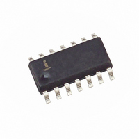
X5648S14I-2.7 Intersil, X5648S14I-2.7 Datasheet

X5648S14I-2.7
Specifications of X5648S14I-2.7
Related parts for X5648S14I-2.7
X5648S14I-2.7 Summary of contents
Page 1
... All other trademarks mentioned are the property of their respective owners. X5648, X5649 (Replaces X25648, X25649) FN8136.0 detection circuitry protects the CC falls below a minimum CC thresholds are available, TRIP RESET/RESET X5648 = RESET X5649 = RESET | Intersil (and design registered trademark of Intersil Americas Inc. Copyright Intersil Americas Inc. 2005. All Rights Reserved ...
Page 2
PIN CONFIGURATION 8-Lead PDIP X5648/ PIN DESCRIPTION Pin Pin (PDIP) (SOIC) Name SCK ...
Page 3
PRINCIPLES OF OPERATION Power-on Reset Application of power to the X5648/X5649 activates a power-on reset circuit. This circuit goes active at about 1V and pulls the RESET/RESET pin active. This signal prevents the system microprocessor from starting to operate with ...
Page 4
Figure 3. V Programming Sequence Flow Chart TRIP New V Applied = CC Old V Applied + Error CC Emax = Maximum Desired Error 4 X5648, X5649 V Programming TRIP Execute Reset V TRIP Sequence Set Applied ...
Page 5
... Program SPI SERIAL MEMORY The memory portion of the device is a CMOS serial EEPROM array with Intersil’s block lock protection. The array is internally organized The device features a Serial Peripheral Interface (SPI) and software proto- col allowing operation on a simple four-wire bus. ...
Page 6
Table 2. Block Protect Matrix WREN CMD Status Register WEL WPEN The Write Enable Latch (WEL) bit indicates the sta- tus of the write enable latch. When WEL = 1, the latch ...
Page 7
Figure 5. Read EEPROM Array Sequence SCK Instruction SI High Impedance SO Write Sequence Prior to any attempt to write data into the device, the Write Enable Latch (WEL) must first be set by issuing ...
Page 8
Figure 6. Read Status Register Sequence CS 0 SCK SI High Impedance SO Figure 7. Write Enable Latch Sequence CS SCK X5648, X5649 ...
Page 9
Figure 8. Write Sequence SCK Instruction SCK Data Byte Figure 9. Status Register Write Sequence CS 0 SCK ...
Page 10
ABSOLUTE MAXIMUM RATINGS Temperature under bias ................... -65°C to +135°C Storage temperature ........................ -65°C to +150°C Voltage on any Pin with respect to V D.C. Output Current ............................................. 5mA Lead temperature (soldering, 10 seconds) ........ 300°C RECOMMENDED OPERATING CONDITIONS Temperature ...
Page 11
EQUIVALENT A.C. LOAD CIRCUIT 2.06kΩ Output RESET/RESET 3.03kΩ 100pF A.C. CHARACTERISTICS (Over recommended operating conditions, unless otherwise specified) Serial Input Timing Symbol f Clock frequency SCK t Cycle time CYC t CS lead time LEAD t ...
Page 12
Serial Output Timing Symbol f Clock frequency SCK t Output disable time DIS t Output valid from clock low V t Output hold time HO (3) t Output rise time RO (3) t Output fall time FO Notes: (3) This ...
Page 13
RESET Output Timing Symbol V Reset trip point voltage, X5648-4.5A, X5648-4.5A TRIP Reset trip point voltage, X5648, X5649 Reset trip point voltage, X5648-2.7A, X5649-2.7A Reset trip point voltage, X5648-2.7, X5649-2 hysteresis (HIGH to LOW vs. LOW to HIGH ...
Page 14
V Reset Conditions TRIP SCK > Programmed V CC TRIP V Programming Specifications V TRIP Parameter t SCK V program voltage setup time VPS TRIP t SCK V program voltage ...
Page 15
TYPICAL PERFORMANCE V Supply Current vs. Temperature ( Watchdog Timer Watchdog Timer Watchdog Timer Off ( -40 25 Temp (°C) V vs. Temperature (programmed at ...
Page 16
PACKAGING INFORMATION Half Shoulder Width On All End Pins Optional .073 (1.84) Typ. 0.010 (0.25) NOTE: 1. ALL DIMENSIONS IN INCHES (IN PARENTHESES IN MILLIMETERS) 2. PACKAGE DIMENSIONS EXCLUDE MOLDING FLASH 16 X5648, X5649 8-Lead Plastic Dual In-Line Package Type ...
Page 17
PACKAGING INFORMATION Pin 1 Index Pin 1 0.014 (0.35) 0.020 (0.51) 0.336 (8.55) 0.345 (8.75) (4X) 7° 0.050 (1.27) 0.010 (0.25) 0.020 (0.50) 0° - 8° 0.016 (0.410) 0.037 (0.937) NOTE: ALL DIMENSIONS IN INCHES (IN PARENTHESES IN MILLIMETERS) 17 ...
Page 18
... TRIP AN = 2.7V to 5.5V, 0°C to +70° 2.7V to 5.5V, -40°C to +85° 2.7V to 5.5V, -40°C to +85°C, V Part Number RESET (Active HIGH) X5649P-4.5A X5649S14-4.5A X5649S14I-4.5A X5648P X5649P X5648S14 X5649S14 X5648S14I X5649S14I X5649S14-2.7A X5649S14-2.7 = 4.25-4.5 TRIP = 4.5-4.75 = 4.25-4.5 = 4.5-4.75 TRIP = 2.55-2.7 = 2.85-3.0 TRIP = 2 ...


