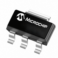
MCP1804T-3302I/DB Microchip Technology, MCP1804T-3302I/DB Datasheet - Page 19

MCP1804T-3302I/DB
Manufacturer Part Number
MCP1804T-3302I/DB
Description
IC REG LDO 3.3V 150MA SOT223-3
Manufacturer
Microchip Technology
Datasheet
1.MCP1804T-C002IOT.pdf
(38 pages)
Specifications of MCP1804T-3302I/DB
Package / Case
SOT-223 (3 leads + Tab), SC-73, TO-261
Regulator Topology
Positive Fixed
Voltage - Output
3.3V
Voltage - Input
Up to 28V
Voltage - Dropout (typical)
1.3V @ 100mA
Number Of Regulators
1
Current - Output
150mA (Min)
Operating Temperature
-40°C ~ 85°C
Mounting Type
Surface Mount
Input Voltage Max
28 V
Output Voltage
1.8 V
Output Voltage Tolerance
+/- 2 %
Dropout Voltage (max)
710 V
Output Current
150 mA
Line Regulation
0.05 %/V
Load Regulation
275 mV
Maximum Power Dissipation
300 mW
Maximum Operating Temperature
+ 85 C
Mounting Style
SMD/SMT
Minimum Operating Temperature
- 40 C
Lead Free Status / RoHS Status
Lead free / RoHS Compliant
Current - Limit (min)
-
Lead Free Status / Rohs Status
Lead free / RoHS Compliant
Other names
MCP1804T-3302I/DBTR
Available stocks
Company
Part Number
Manufacturer
Quantity
Price
4.0
4.1
A portion of the LDO output voltage is fed back to the
internal error amplifier and compared with the precision
internal bandgap reference. The error amplifier output
will adjust the amount of current that flows through the
P-Channel pass transistor, thus regulating the output
voltage to the desired value. Any changes in input
voltage or output current will cause the error amplifier
to respond and adjust the output voltage to the target
voltage (refer to
4.2
The MCP1804 internal circuitry monitors the amount of
current flowing through the P-Channel pass transistor.
In the event that the load current reaches the current
limiter level of 200 mA (typical), the current limiter
circuit will operate and the output voltage will drop. As
the output voltage drops, the internal current foldback
circuit will further reduce the output voltage causing the
output current to decrease. When the output is shorted,
a typical output current of 50 mA flows.
4.3
The SHDN input is used to turn the LDO output voltage
on and off. When the SHDN input is at a logic-high
level, the LDO output voltage is enabled. When the
SHDN input is pulled to a logic-low level, the LDO
output voltage is disabled and the LDO enters a low
quiescent current shutdown state where the typical
quiescent current is 0.01 µA. The SHDN pin does not
have an internal pullup or pulldown resistor. Therefore
the SHDN pin must be pulled either high or low to
prevent the device from becoming unstable. The
internal device current will increase when the device is
operational and current flows through the pullup or
pull-down resistor to the SHDN pin internal logic. The
SHDN pin internal logic is equivalent to an inverter
input.
© 2009 Microchip Technology Inc.
DETAILED DESCRIPTION
Output Regulation
Overcurrent
Shutdown
Figure
4-1).
4.4
of 0.1 µF to 1.0 µF for output voltage stability. Ceramic
capacitors are recommended because of their size,
cost and environmental robustness qualities.
Aluminum-electrolytic and tantalum capacitors can be
used on the LDO output as well. The output capacitor
should be located as close to the LDO output as is
practical. Ceramic materials X7R and X5R have low
temperature coefficients.
Larger LDO output capacitors can be used with the
MCP1804 to improve dynamic performance and power
supply
electrolytic capacitors are not recommended for low
temperature applications of < -25°C.
4.5
Low input source impedance is necessary for the LDO
output to operate properly. When operating from
batteries, or in applications with long lead length
(> 10 inches) between the input source and the LDO,
some input capacitance is recommended. A minimum
of 0.1 µF to 1.0 µF is recommended for most
applications.
For
requirements, the input capacitance of the LDO is very
important. The input capacitance provides the LDO
with a good local low-impedance source to pull the
transient currents from in order to respond quickly to
the output load step. For good step response
performance, the input capacitor should be of
equivalent or higher value than the output capacitor.
The capacitor should be placed as close to the input of
the LDO as is practical. Larger input capacitors will also
help reduce any high-frequency noise on the input and
output of the LDO and reduce the effects of any
inductance that exists between the input source
voltage and the input capacitance of the LDO.
4.6
The MCP1804 thermal shutdown circuitry protects the
device when the internal junction temperature reaches
the typical thermal limit value of +150°C. The thermal
limit shuts off the output drive transistor. Device output
will resume when the internal junction temperature falls
below the thermal limit value by an amount equal to the
thermal limit hysteresis value of +25°C.
The MCP1804 requires a minimum output capacitance
applications
ripple
Output Capacitor
Input Capacitor
Thermal Shutdown
rejection
that
have
performance.
MCP1804
output
DS22200B-page 19
step
Aluminum-
load


