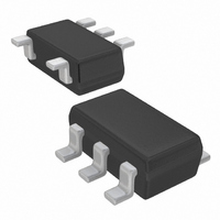
XC6701B332MR Torex Semiconductor Ltd, XC6701B332MR Datasheet - Page 11

XC6701B332MR
Manufacturer Part Number
XC6701B332MR
Description
IC VREG LDO 3.3V HS SOT-25
Manufacturer
Torex Semiconductor Ltd
Datasheet
1.XC6701B502MR.pdf
(35 pages)
Specifications of XC6701B332MR
Regulator Topology
Positive Fixed
Voltage - Output
3.3V
Voltage - Input
Up to 28V
Voltage - Dropout (typical)
1.3V @ 100mA
Number Of Regulators
1
Current - Output
150mA (Min)
Current - Limit (min)
200mA
Operating Temperature
-40°C ~ 85°C
Mounting Type
Surface Mount
Package / Case
SOT-23-5, SC-74A, SOT-25
Primary Input Voltage
5.3V
Output Voltage
3.3V
Dropout Voltage Vdo
260mV
No. Of Pins
5
Output Current
150mA
Voltage Regulator Case Style
SOT-25
Operating Temperature Range
-40°C To +85°C
Output Voltage Fixed
3.3V
Rohs Compliant
Yes
Lead Free Status / RoHS Status
Lead free / RoHS Compliant
Other names
893-1102-2
Available stocks
Company
Part Number
Manufacturer
Quantity
Price
Company:
Part Number:
XC6701B332MR-G
Manufacturer:
SAMTEC
Quantity:
2
Part Number:
XC6701B332MR-G
Manufacturer:
TOREX
Quantity:
20 000
■ NOTES ON USE
1. For temporary, transitional voltage drop or voltage rising phenomenon, the IC is liable to malfunction should the ratings be
2. Where wiring impedance is high, operations may become unstable due to the noise and/or phase lag depending on output
3. Phase compensation inside the IC is performed in the XC6701 series. Therefore, an abnormal oscillation does not occur
4. When the IC is operated with no load, the output voltage may increase in the high temperature beyond operating range.
5. Torex places an importance on improving our products and its reliability.
■ OPERATIONAL EXPLANATION
<Output Voltage Control>
<Short-Circuit Protection>
<CE Pin>
<Thermal Shutdown>
<Minimum Operating Voltage>
The voltage divided by resistors R1 & R2 is compared with the internal reference voltage by the error amplifier. The
P-channel MOSFET, which is connected to the V
voltage at the V
circuit and thermal protection circuit operate in relation to the level of output current and heat generation. Further, the IC’s
internal circuitry can be shutdown via the CE pin’s signal.
The XC6701 series includes a current fold-back circuit as a short circuit protection. When the load current reaches the
current limit level, the current fold-back circuit operates and output voltage drops. The output voltage drops further and
output current decreases. When the output pin is shorted, a current of about 30mA flows.
The IC’s internal circuitry can be shutdown via the signal from the CE pin with the XC6701B series. In shutdown mode,
output at the V
become unstable with the CE pin open. We suggest that you use this IC with either a V
the CE pin. If this IC is used with the correct specifications for the CE pin, the operational logic is fixed and the IC will
operate normally. However, supply current may increase as a result of through current in the IC’s internal circuitry if a
medium voltage is applied.
When the junction temperature of the built-in driver transistor reaches the temperature limit level (150℃ TYP.), the thermal
protection circuit operates and the driver transistor will be set to OFF. The IC resumes its operation when the thermal
shutdown function is released and the IC’s operation is automatically restored because the junction temperature drops to
the level of the thermal shutdown release voltage.
For the stable operation of the IC, over 2.0V of input voltage is necessary. The output voltage may not be generated
normally if the input voltage is less than 2.0V.
exceeded.
current. Please strengthen V
even if there is no output capacitor C
is required for input stability. Also, the output voltage fluctuation such as under shoot or over shoot, which occurs
because of the load change can be controlled by placing the output capacitor C
pin and V
with a shorter wiring.
However, by any possibility, we would request user fail-safe design and post-aging treatment on system or equipment.
SS
pin. The input capacitor (C
OUT
OUT
pin will be pulled down by R1 and R2 to the V
pin is controlled and stabilized by a system of negative feedback. The current limit circuit, short protect
IN
and V
L
. An input capacitor C
SS
IN
wiring in particular.
) and the output capacitor (C
OUT
pin, is then driven by the subsequent output signal. The output
IN
around 0.1μF~1.0μF between the V
SS
level. Note that as the XC6701B series’ operations will
L
) should be placed to the IC as close as possible
L
R1
R2
around 0.1μF~1.0μF between the V
IN
voltage or a V
IN
pin and the V
SS
voltage input at
XC6701
11/35
Series
SS
OUT
pin


