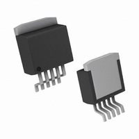
LP3891ES-1.5/NOPB National Semiconductor, LP3891ES-1.5/NOPB Datasheet - Page 4

LP3891ES-1.5/NOPB
Manufacturer Part Number
LP3891ES-1.5/NOPB
Description
IC REG LDO 0.8A 1.5V TO-263-5
Manufacturer
National Semiconductor
Datasheet
1.LP3891ES-1.2NOPB.pdf
(11 pages)
Specifications of LP3891ES-1.5/NOPB
Regulator Topology
Positive Fixed
Voltage - Output
1.5V
Voltage - Input
Up to 5.5V
Voltage - Dropout (typical)
0.1V @ 800mA
Number Of Regulators
1
Current - Output
800mA
Operating Temperature
-40°C ~ 125°C
Mounting Type
Surface Mount
Package / Case
TO-263-5, D²Pak (5 leads + Tab), TO-263BA
Lead Free Status / RoHS Status
Lead free / RoHS Compliant
Current - Limit (min)
-
Other names
*LP3891ES-1.5
*LP3891ES-1.5/NOPB
LP3891ES-1.5
*LP3891ES-1.5/NOPB
LP3891ES-1.5
Available stocks
Company
Part Number
Manufacturer
Quantity
Price
Company:
Part Number:
LP3891ES-1.5/NOPB
Manufacturer:
National Semiconductor
Quantity:
135
www.national.com
AC Parameters
PSRR (V
PSRR
(V
e
n
Electrical Characteristics
over the full operating temperature range. Unless otherwise specified: V
C
Note 1: Absolute maximum ratings indicate limits beyond which damage to the component may occur. Operating ratings indicate conditions for which the device
is intended to be functional, but do not guarantee specific performance limits. For guaranteed specifications, see Electrical Characteristics. Specifications do not
apply when operating the device outside of its rated operating conditions.
Note 2: At elevated temperatures, device power dissipation must be derated based on package thermal resistance and heatsink thermal values. θ
devices is 65˚C/W if no heatsink is used. If the TO-220 device is attached to a heatsink, a θ
approximately 40˚C/W if soldered down to a copper plane which is at least 1.5 square inches in area. θ
If power dissipation causes the junction temperature to exceed specified limits, the device will go into thermal shutdown.
Note 3: The human body model is a 100 pF capacitor discharged through a 1.5k resistor into each pin.
Note 4: Typical numbers represent the most likely parametric norm for 25˚C operation.
Note 5: Limits are guaranteed through testing, statistical correlation, or design.
Note 6: If used in a dual-supply system where the regulator load is returned to a negative supply, the output pin must be diode clamped to ground.
Note 7: Output voltage line regulation is defined as the change in output voltage from nominal value resulting from a change in input voltage.
Note 8: Output voltage load regulation is defined as the change in output voltage from nominal value as the load current increases from no load to full load.
Note 9: Dropout voltage is defined as the minimum input to output differential required to maintain the output with 2% of nominal value. The PSOP-8 package
devices have a slightly higher dropout voltage due to increased band wire resistance.
Note 10: The machine model is a 220 pF capacitor discharged directly into each pin. The machine model ESD rating of pin 5 is 100V.
BIAS
Symbol
OUT
)
= 10 µF, V
IN
)
Ripple Rejection for V
Voltage
Ripple Rejection for V
Voltage
Output Noise Density
Output Noise Voltage
S/D
= V
BIAS
Parameter
. (Continued)
IN
BIAS
Input
Limits in standard typeface are for T
V
V
V
V
f = 120 Hz
BW = 10 Hz − 100 kHz, V
1.8V
BW = 300 Hz − 300 kHz, V
= 1.8V
IN
IN
BIAS
BIAS
= V
= V
= V
= V
OUT
OUT
OUT
OUT
Conditions
+1V, f = 120 Hz
+ 1V, f = 1 kHz
4
+ 3V, f = 120 Hz
+ 3V, f = 1 kHz
IN
= V
J-S
OUT
OUT
O
value of 4˚C/W can be assumed. θ
J
(NOM) + 1V, V
J-A
=
= 25˚C, and limits in boldface type apply
value for typical PSOP-8 PC board mounting is 166˚C/W.
(Note
MIN
5)
BIAS
(Note 4)
Typical
150
80
65
70
65
90
= 4.5V, I
1
J-A
(Note
L
MAX
5)
for TO-263 devices is
= 10 mA, C
J-A
µV/root−Hz
µV (rms)
for TO-220
Units
IN
dB
=


