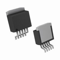
LP3891ES-1.5/NOPB National Semiconductor, LP3891ES-1.5/NOPB Datasheet - Page 8

LP3891ES-1.5/NOPB
Manufacturer Part Number
LP3891ES-1.5/NOPB
Description
IC REG LDO 0.8A 1.5V TO-263-5
Manufacturer
National Semiconductor
Datasheet
1.LP3891ES-1.2NOPB.pdf
(11 pages)
Specifications of LP3891ES-1.5/NOPB
Regulator Topology
Positive Fixed
Voltage - Output
1.5V
Voltage - Input
Up to 5.5V
Voltage - Dropout (typical)
0.1V @ 800mA
Number Of Regulators
1
Current - Output
800mA
Operating Temperature
-40°C ~ 125°C
Mounting Type
Surface Mount
Package / Case
TO-263-5, D²Pak (5 leads + Tab), TO-263BA
Lead Free Status / RoHS Status
Lead free / RoHS Compliant
Current - Limit (min)
-
Other names
*LP3891ES-1.5
*LP3891ES-1.5/NOPB
LP3891ES-1.5
*LP3891ES-1.5/NOPB
LP3891ES-1.5
Available stocks
Company
Part Number
Manufacturer
Quantity
Price
Company:
Part Number:
LP3891ES-1.5/NOPB
Manufacturer:
National Semiconductor
Quantity:
135
www.national.com
Application Hints
EXTERNAL CAPACITORS
To assure regulator stability, input and output capacitors are
required as shown in the Typical Application Circuit.
OUTPUT CAPACITOR
At least 10µF of output capacitance is required for stability
(the amount of capacitance can be increased without limit).
The output capacitor must be located less than 1cm from the
output pin of the IC and returned to a clean analog ground.
The ESR (equivalent series resistance) of the output capaci-
tor must be within the "stable" range as shown in the graph
below over the full operating temperature range for stable
operation.
Tantalum capacitors are recommended for the output as
their ESR is ideally suited to the part’s requirements and the
ESR is very stable over temperature. Aluminum electrolytics
are not recommended because their ESR increases very
rapidly at temperatures below 10˚C. Aluminum caps can only
be used in applications where lower temperature operation
is not required.
A second problem with Al caps is that many have ESR’s
which are only specified at low frequencies. The typical loop
bandwidth of a linear regulator is a few hundred kHz to
several MHz. If an Al cap is used for the output cap, it must
be one whose ESR is specified at a frequency of 100 kHz or
more.
Because the ESR of ceramic capacitors is only a few milli
Ohms, they are not suitable for use as output capacitors on
LP389X devices. The regulator output can tolerate ceramic
capacitance totaling up to 15% of the amount of Tantalum
capacitance connected from the output to ground.
INPUT CAPACITOR
The input capacitor must be at least 10 µF, but can be
increased without limit. It’s purpose is to provide a low
source impedance for the regulator input. Ceramic capaci-
tors work best for this, but Tantalums are also very good.
There is no ESR limitation on the input capacitor (the lower,
the better). Aluminum electrolytics can be used, but their
ESR increase very quickly at cold temperatures. They are
not recommended for any application where temperatures
go below about 10˚C.
Minimum ESR vs Output Load Current
20069531
8
BIAS CAPACITOR
The 0.1µF capacitor on the bias line can be any good quality
capacitor (ceramic is recommended).
BIAS VOLTAGE
The bias voltage is an external voltage rail required to get
gate drive for the N-FET pass transistor. Bias voltage must
be in the range of 4.5 - 6V to assure proper operation of the
part.
UNDER VOLTAGE LOCKOUT
The bias voltage is monitored by a circuit which prevents the
regulator output from turning on if the bias voltage is below
approximately 4V.
SHUTDOWN OPERATION
Pulling down the shutdown (S/D) pin will turn-off the regula-
tor. Pin S/D must be actively terminated through a pull-up
resistor (10 kΩ to 100 kΩ) for a proper operation. If this pin
is driven from a source that actively pulls high and low (such
as a CMOS rail to rail comparator), the pull-up resistor is not
required. This pin must be tied to Vin if not used.
POWER DISSIPATION/HEATSINKING
A heatsink may be required depending on the maximum
power dissipation and maximum ambient temperature of the
application. Under all possible conditions, the junction tem-
perature must be within the range specified under operating
conditions. The total power dissipation of the device is given
by:
P
where I
The maximum allowable temperature rise (T
on the maximum ambient temperature (T
cation, and the maximum allowable junction temperature
(T
T
The maximum allowable value for junction to ambient Ther-
mal Resistance, θ
θ
These parts are available in TO-220 and TO-263 packages.
The thermal resistance depends on amount of copper area
or heat sink, and on air flow. If the maximum allowable value
of θ
and ≥ 60 ˚C/W for TO-263 package no heatsink is needed
since the package can dissipate enough heat to satisfy these
requirements. If the value for allowable θ
limits, a heat sink is required.
HEATSINKING TO-220 PACKAGE
The thermal resistance of a TO220 package can be reduced
by attaching it to a heat sink or a copper plane on a PC
board. If a copper plane is to be used, the values of θ
be same as shown in next section for TO263 package.
The heatsink to be used in the application should have a
heatsink to ambient thermal resistance,
θ
In this equation, θ
to the surface of the heat sink and θ
tance from the junction to the surface of the case. θ
about 3˚C/W for a TO220 package. The value for θ
pends on method of attachment, insulator, etc. θ
between 1.5˚C/W to 2.5˚C/W. If the exact value is unknown,
2˚C/W can be assumed.
JA
HA
Rmax
D
Jmax
= (V
≤ θ
= T
JA
):
= T
JA
calculated above is ≥ 60 ˚C/W for TO-220 package
Rmax
GND
IN
−V
− θ
Jmax
is the operating ground current of the device.
OUT
/ P
CH
− T
D
)I
− θ
OUT
Amax
CH
JA
JC
, can be calculated using the formula:
is the thermal resistance from the case
+ (V
.
IN
)I
GND
JC
is the thermal resis-
JA
Amax
falls below these
Rmax
) of the appli-
) depends
CH
CH
JA
varies
JC
de-
will
is


