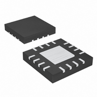
MAX8556ETE+ Maxim Integrated Products, MAX8556ETE+ Datasheet - Page 7

MAX8556ETE+
Manufacturer Part Number
MAX8556ETE+
Description
IC REG LDO 4A 16-TQFN
Manufacturer
Maxim Integrated Products
Datasheet
1.MAX8556EVKIT.pdf
(10 pages)
Specifications of MAX8556ETE+
Regulator Topology
Positive Adjustable
Voltage - Output
0.5 ~ 3.4 V
Voltage - Input
1.43 ~ 3.6 V
Voltage - Dropout (typical)
0.1V @ 4A
Number Of Regulators
1
Current - Output
4A
Operating Temperature
-40°C ~ 85°C
Mounting Type
Surface Mount
Package / Case
16-TQFN Exposed Pad
Input Voltage Max
3.6 V
Output Voltage
3.4 V
Dropout Voltage (max)
200 mV
Output Current
4 A
Load Regulation
0.1 %/A
Voltage Regulation Accuracy
0.1 %
Maximum Power Dissipation
2666.7 mW
Maximum Operating Temperature
+ 85 C
Mounting Style
SMD/SMT
Minimum Operating Temperature
- 40 C
Lead Free Status / RoHS Status
Lead free / RoHS Compliant
Current - Limit (min)
-
Lead Free Status / Rohs Status
Lead free / RoHS Compliant
The MAX8556/MAX8557 low-dropout linear regulators
are capable of delivering up to 4A from low-input volt-
age supplies ranging from 1.425V to 3.6V with only
200mV of dropout (max). The pMOS output stage can
be driven from input voltages down to 1.425V without
sacrificing stability or transient performance. Supply
current is not a significant function of load or input head-
room because this regulator has a pMOS output device.
The MAX8556/MAX8557 are fully protected from an out-
put short circuit by current-limiting and thermal-overload
circuitry. The low-power shutdown mode reduces sup-
ply current to 0.2µA (typ) to maximize battery life in
portable applications. The MAX8556 includes an open-
drain power-OK signal (POK) that goes high when the
regulator output is within ±10% of its nominal output
voltage. The MAX8557 includes an open-drain power-
on-reset output (POR) that goes high 140ms after the
output has risen above 90% of its nominal value.
The MAX8556/MAX8557 feature a 25mΩ p-channel
MOSFET pass transistor. Unlike similar designs using
pnp pass transistors, p-channel MOSFETs require no
base drive, which reduces quiescent current; pnp-
based regulators also waste considerable current in
dropout when the pass transistor saturates, and use
high base-drive currents under large loads. The
MAX8556/MAX8557 do not suffer from these problems
and consume only 800µA (typ) of quiescent current
under heavy loads, as well as in dropout.
The MAX8556/MAX8557 are fully protected from output
short circuits through current-limiting and thermal-over-
load circuitry. When the output is shorted to ground, the
output current is foldback limited to 3A (max). Under
these conditions, the device quickly heats up. When
the junction temperature reaches +160°C, the thermal-
overload circuitry turns off the output, allowing the
device to cool. When the junction cools to +115°C, the
output turns back on and attempts to establish regula-
tion. Current limiting and thermal protection continue
until the fault is removed.
Short-Circuit/Thermal Fault Protection
Internal p-Channel Pass Transistor
_______________________________________________________________________________________
Detailed Description
4A Ultra-Low-Input-Voltage
The MAX8556/MAX8557 feature a low-power shutdown
mode that reduces quiescent current to 0.2µA (typ).
Drive EN low to disable the voltage reference, error
amplifier, gate-drive circuitry, and pass transistor, and
pull the output low with 5kΩ impedance. Drive EN high
or connect to IN for normal operation.
The MAX8556 features a power-OK (POK) output to
indicate the status of the output. POK is high impedance
when the regulator output is within ±10% of its nominal
output voltage. If the output voltage falls/rises outside
this range or the IC experiences thermal fault, POK is
internally pulled low. This open-drain output requires an
external pullup resistor to V
below 3.6V. For glitch immunity, an internal delay circuit
prevents the output from switching for 50µs (typ) after
the trip threshold is initially reached. POK is low when
the IC is in shutdown mode.
The MAX8557 features a power-on reset output that
goes high impedance 140ms (typ) after the output
reaches 90% of its nominal value. This open-drain out-
put requires an external pullup resistor to V
logic supply less than 3.6V. When the output falls below
90% of the nominal output voltage or the IC experi-
ences a thermal fault, POR immediately transitions low.
POR is low when the IC is in shutdown mode.
The maximum power dissipation depends on the ther-
mal resistance of the IC package and the circuit board,
the temperature difference between the die junction and
ambient air, and the rate of ambient airflow. The power
dissipated by the IC is P = I
PCB layout can increase the allowed power dissipation
by dissipating heat in the board instead of the package.
See the Thermal Considerations in PCB Layout section
for more details.
Operating Region and Power Dissipation
Power-OK Output (POK, MAX8556 Only)
Power-On Reset (POR, MAX8557 Only)
LDO Regulators
OUT
IN
or another logic supply
x (V
Shutdown Mode
IN
- V
IN
OUT
or another
). Proper
7


