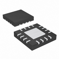
MAX8556ETE+ Maxim Integrated Products, MAX8556ETE+ Datasheet - Page 9

MAX8556ETE+
Manufacturer Part Number
MAX8556ETE+
Description
IC REG LDO 4A 16-TQFN
Manufacturer
Maxim Integrated Products
Datasheet
1.MAX8556EVKIT.pdf
(10 pages)
Specifications of MAX8556ETE+
Regulator Topology
Positive Adjustable
Voltage - Output
0.5 ~ 3.4 V
Voltage - Input
1.43 ~ 3.6 V
Voltage - Dropout (typical)
0.1V @ 4A
Number Of Regulators
1
Current - Output
4A
Operating Temperature
-40°C ~ 85°C
Mounting Type
Surface Mount
Package / Case
16-TQFN Exposed Pad
Input Voltage Max
3.6 V
Output Voltage
3.4 V
Dropout Voltage (max)
200 mV
Output Current
4 A
Load Regulation
0.1 %/A
Voltage Regulation Accuracy
0.1 %
Maximum Power Dissipation
2666.7 mW
Maximum Operating Temperature
+ 85 C
Mounting Style
SMD/SMT
Minimum Operating Temperature
- 40 C
Lead Free Status / RoHS Status
Lead free / RoHS Compliant
Current - Limit (min)
-
Lead Free Status / Rohs Status
Lead free / RoHS Compliant
How much power the package can dissipate strongly
depends on the mounting method of the IC to the PCB
and the copper area for cooling. Using the JEDEC test
standard, the maximum power dissipation allowed in
the package is 2667mW. This data is obtained with
+70°C ambient temperature and +150°C maximum
junction temperature. The test board has dimensions of
3in x 3in with four layers of 2oz copper and FR-4 mater-
ial with 62mil finished thickness. Nine thermal vias are
used under the thermal paddle with a diameter of 12mil
and 1mil plated copper thickness. Top and bottom lay-
ers are used to route the traces. Two middle layers are
solid copper and isolated from the nine thermal vias.
More power dissipation can be handled by the pack-
age if great attention is given during PCB layout. For
example, using the top and bottom copper as a
heatsink and connecting the thermal vias to one of the
middle layers (GND) transfers the heat from the pack-
age into the board more efficiently, resulting in lower
junction temperature at high power dissipation in some
MAX8556/MAX8557 applications. Furthermore, the sol-
der mask around the IC area on both top and bottom
layers can be removed to radiate the heat directly into
the air. The maximum allowable power dissipation in
the IC is as follows:
TRANSISTOR COUNT: 3137
PROCESS: BiCMOS
P
MAX
_______________________________________________________________________________________
=
Thermal Considerations
(
T
J MAX
θ
Chip Information
(
JC
+
)
θ
CA
−
T
in PCB Layout
A
)
4A Ultra-Low-Input-Voltage
For the latest package outline information and land patterns, go
to www.maxim-ic.com/packages. Note that a “+”, “#”, or “-” in
the package code indicates RoHS status only. Package draw-
ings may show a different suffix character, but the drawing per-
tains to the package regardless of RoHS status.
where T
(+150°C), T
(1.7°C/W for the 16-pin TQFN) is the thermal resistance
from the junction to the case, and θ
resistance from the case to the surrounding air through
the PCB, copper traces, and the package materials.
θ
be modified to increase the maximum power dissipa-
tion. The TQFN package has an exposed thermal pad
on its underside. This pad provides a low thermal resis-
tance path for heat transfer into the PCB. This low ther-
mally resistive path carries a majority of the heat away
from the IC. The PCB is effectively a heatsink for the IC.
The exposed paddle should be connected to a large
ground plane for proper thermal and electrical perfor-
mance. The minimum size of the ground plane is
dependent upon many system variables. To create an
efficient path, the exposed paddle should be soldered
to a thermal landing, which is connected to the ground
plane by thermal vias. The thermal landing should be at
least as large as the exposed paddle and can be made
larger depending on the amount of free space from the
exposed paddle to the other pin landings.
A sample layout is available on the MAX8556 evalua-
tion kit to speed designs.
CA
PACKAGE TYPE
16 TQFN-EP
is directly related to system level variables and can
J(MAX)
A
is the ambient air temperature, θ
is the maximum junction temperature
LDO Regulators
PACKAGE CODE
Package Information
T1655+2
CA
DOCUMENT NO.
is the thermal
21-0140
JC
9


