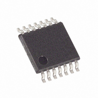
MAX8528EUD+ Maxim Integrated Products, MAX8528EUD+ Datasheet - Page 7

MAX8528EUD+
Manufacturer Part Number
MAX8528EUD+
Description
IC REG LDO 2A 14-TSSOP
Manufacturer
Maxim Integrated Products
Datasheet
1.MAX8526EVKIT.pdf
(10 pages)
Specifications of MAX8528EUD+
Regulator Topology
Positive Adjustable
Voltage - Output
0.5 ~ 3.4 V
Voltage - Input
1.43 ~ 3.6 V
Voltage - Dropout (typical)
0.1V @ 2A
Number Of Regulators
1
Current - Output
2A
Current - Limit (min)
3.2A
Operating Temperature
-40°C ~ 85°C
Mounting Type
Surface Mount
Package / Case
14-TSSOP Exposed Pad, 14-eTSSOP 14-HTSSOP
Number Of Outputs
1
Polarity
Positive
Input Voltage Max
3.6 V
Output Voltage
0.5 V to 3.4 V
Output Type
Adjustable
Dropout Voltage (max)
0.2 V at 2 A
Output Current
2 A
Line Regulation
0.15 % / V
Load Regulation
0.08 % / A
Voltage Regulation Accuracy
0.6 %
Maximum Power Dissipation
1.7 W
Maximum Operating Temperature
+ 85 C
Mounting Style
SMD/SMT
Minimum Operating Temperature
- 40 C
Lead Free Status / RoHS Status
Lead free / RoHS Compliant
The MAX8526/MAX8527/MAX8528 are low-input, low-
dropout, PMOS regulators capable of delivering up to
2A of output current with as little as 200mV of head-
room from input to output. The PMOS output stage can
be driven from input voltages down to +1.425V without
sacrificing stability or transient performance. Since this
regulator has a PMOS output device, supply current is
not a significant function of load or input headroom.
The MAX8526/MAX8527/MAX8528 feature a 50mΩ
(typ) p-channel MOSFET pass transistor. Unlike similar
designs using pnp pass transistors, p-channel MOSFETs
require no base drive, which reduces quiescent current.
pnp-based regulators also waste considerable current in
dropout when the pass transistor saturates, and use high
base-drive currents under large loads. The MAX8526/
MAX8527/MAX8528 do not suffer from these problems
and consume only 500µA (typ) of quiescent current
under heavy loads, as well as in dropout.
The MAX8526/MAX8527/MAX8528 are fully protected
from a short circuit at the output through current-limit-
ing and thermal-overload circuitry. In the fault condition
when the output is shorted to ground, the output cur-
rent is limited to 4A. Under these conditions, the part
quickly heats up. When the junction temperature reach-
es +165°C, the thermal-overload circuitry turns off the
output, allowing the part to cool down. When the junc-
tion temperature cools to +150°C, the output turns
back on and tries to reestablish regulation. Current
limiting and thermal protection continue until the fault is
removed. For continuous operation, do not exceed the
absolute maximum junction temperature rating of
T
Figure 1. Typical Application Circuit
J
2.2µF
= +150°C.
+1.425V TO +3.6V
SHUTDOWN
100kΩ*
ENABLE
Short-Circuit/Thermal Fault Protection
*FOR MAX8527 AND MAX8528
Internal p-Channel Pass Transistor
IN
IN
IN
IN
POK (MAX8527) OR
POR (MAX8528)
EN
_______________________________________________________________________________________
Detailed Description
MAX8526
MAX8527
MAX8528
OUT
OUT
GND
OUT
OUT
FB
ADJUSTABLE
R1
R2
0.2V Dropout LDO Regulators
OUTPUT
10µF
1.425V to 3.6V Input, 2A,
The MAX8526/MAX8527/MAX8528 feature an
adjustable output voltage from 0.5V to 3.4V, using two
external resistors connected as a voltage-divider to FB
as shown in Figure 1. The output voltage is set by the
following equation:
where typically V
mize quiescent current, accuracy, and high-frequency
power-supply rejection. To simplify resistor selection:
Inherent soft-start limits inrush current. Peak inrush cur-
rent is dependent on the value of C
calculated as follows:
The MAX8526/MAX8527/MAX8528 include an enable
input. To shut down the device, pull EN to GND. For
normal operation, connect the EN to IN. During shut-
down, an internal 10kΩ resistor pulls down the output.
The MAX8527 features a power-OK output to indicate
the status of the output. POK remains high when the
regulator output is within ±10% of its nominal output
voltage. If the output voltage falls/rises outside this
range, POK transitions low. This open-drain output
requires an external pullup resistor to IN. An internal
delay circuit prevents the POK from switching for 50µs
(typ) after the trip threshold is initially reached. If the
part is in shutdown mode, POK is low.
The MAX8528 features a power-on reset output that
transitions high 150ms (typ) after the output has risen
above 90% of its final value. This open-drain output
requires an external pullup resistor to IN. If the part is in
shutdown mode, falls below 90% of the nominal output
voltage, or experiences a short-circuit/thermal fault,
POR immediately transitions low.
Power-On Reset (POR, MAX8528 Only)
I
INRUSH
Power-OK (POK, MAX8527 Only)
V
OUT
FB
R
=
1
I
= 0.5V. Choose R2 < 5kΩ to opti-
LOAD
=
=
Output Voltage Selection
R
V
2
FB
⎛
⎜
⎝
+
V
⎛
⎜
⎝
V
OUT
1
FB
⎛
⎜
⎝
+
C
OUT
R
-1
R
Shutdown Mode
66
1
2
⎞
⎟
⎠
⎞
⎟
⎠
( )
OUT
µ
F
⎞
⎟
⎠
Soft-Start
and can be
7


