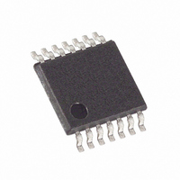
MAX8528EUD+ Maxim Integrated Products, MAX8528EUD+ Datasheet - Page 8

MAX8528EUD+
Manufacturer Part Number
MAX8528EUD+
Description
IC REG LDO 2A 14-TSSOP
Manufacturer
Maxim Integrated Products
Datasheet
1.MAX8526EVKIT.pdf
(10 pages)
Specifications of MAX8528EUD+
Regulator Topology
Positive Adjustable
Voltage - Output
0.5 ~ 3.4 V
Voltage - Input
1.43 ~ 3.6 V
Voltage - Dropout (typical)
0.1V @ 2A
Number Of Regulators
1
Current - Output
2A
Current - Limit (min)
3.2A
Operating Temperature
-40°C ~ 85°C
Mounting Type
Surface Mount
Package / Case
14-TSSOP Exposed Pad, 14-eTSSOP 14-HTSSOP
Number Of Outputs
1
Polarity
Positive
Input Voltage Max
3.6 V
Output Voltage
0.5 V to 3.4 V
Output Type
Adjustable
Dropout Voltage (max)
0.2 V at 2 A
Output Current
2 A
Line Regulation
0.15 % / V
Load Regulation
0.08 % / A
Voltage Regulation Accuracy
0.6 %
Maximum Power Dissipation
1.7 W
Maximum Operating Temperature
+ 85 C
Mounting Style
SMD/SMT
Minimum Operating Temperature
- 40 C
Lead Free Status / RoHS Status
Lead free / RoHS Compliant
The maximum power dissipation depends on the ther-
mal resistance of the IC package and circuit board, the
temperature difference between the die junction and
ambient air, and the rate of airflow. The power dissipat-
ed in the device is P = I
The package features an exposed thermal pad on its
underside. This pad lowers the thermal resistance of
the package by providing a direct heat conduction
path from the die to the PC board.
Additionally, the ground pins (GND) perform the dual
function of providing an electrical connection to system
ground and channeling heat away. Connect the
exposed backside pad and GND to the system ground
using a large pad or ground plane, or multiple vias to
the ground-plane layer.
Capacitors are required at the MAX8526/MAX8527/
MAX8528 inputs and outputs for stable operation over
the full temperature range and with load currents up to
2A. Connect a 2.2µF capacitor between IN and ground
and a 10µF capacitor with low equivalent-series-resis-
tance (ESR) capacitor between OUT and ground for 2A
1.425V to 3.6V Input, 2A,
0.2V Dropout LDO Regulators
8
Operating Region and Power Dissipation
_______________________________________________________________________________________
Applications Information
OUT
Capacitor Selection and
x (V
Regulator Stability
IN
- V
OUT
).
output current. The input capacitor (C
source impedance of the input supply. If input-supply
source impedance is high, place a larger input capaci-
tor close to IN to prevent V
sients. Smaller output capacitors can be used for output
currents less than 2A. Calculate C
The MAX8526/MAX8527/MAX8528 are designed to
operate with low dropout voltages and low quiescent
currents, while still maintaining good noise, transient
response, and AC rejection. See the Typical Operating
Characteristics for a plot of Power-Supply Rejection
Ratio (PSRR) vs. Frequency. When operating from
noisy sources, improved supply-noise rejection and
transient response can be achieved by increasing the
values of the input and output bypass capacitors and
through passive filtering techniques. The MAX8526/
MAX8527/MAX8528 load-transient response graphs
(see the Typical Operating Characteristics ) show two
components of the output response: a DC shift from the
output impedance due to the load current change, and
the transient response. A typical transient overshoot for
a step change in the load current from 20mA to 2A is
45mV. Use larger output ceramic capacitors greater
than 10µF up to 100µF to attenuate the overshoot.
Noise, PSRR, and Transient Response
C
OUT
= I
OUT(max)
IN
sagging due to load tran-
(1µF / 200mA)
OUT
as follows:
IN
) lowers the


