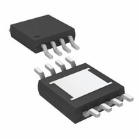
LT3010EMS8E-5#TR Linear Technology, LT3010EMS8E-5#TR Datasheet - Page 4

LT3010EMS8E-5#TR
Manufacturer Part Number
LT3010EMS8E-5#TR
Description
IC REG LDO LIN 5V 50MA 8-MSOP
Manufacturer
Linear Technology
Datasheet
1.LT3010EMS8E-5.pdf
(18 pages)
Specifications of LT3010EMS8E-5#TR
Regulator Topology
Positive Fixed
Voltage - Output
5V
Voltage - Input
Up to 80V
Voltage - Dropout (typical)
0.3V @ 50mA
Number Of Regulators
1
Current - Output
50mA
Current - Limit (min)
60mA
Operating Temperature
-40°C ~ 125°C
Mounting Type
Surface Mount
Package / Case
8-MSOP Exposed Pad, 8-HMSOP, 8-eMSOP
Lead Free Status / RoHS Status
Contains lead / RoHS non-compliant
Available stocks
Company
Part Number
Manufacturer
Quantity
Price
ELECTRICAL CHARACTERISTICS
LT3010/LT3010-5
140°C operating temperature range, otherwise specifi cations are at T
PARAMETER
Dropout Voltage
V
(Notes 4, 5)
GND Pin Current
V
(Notes 4, 6)
Output Voltage Noise
ADJ Pin Bias Current
Shutdown Threshold
SHDN Pin Current
(Note 8)
Quiescent Current in Shutdown V
Ripple Rejection
Current Limit
Input Reverse Leakage Current V
Reverse Output Current
(Note 9)
Note 1: Stresses beyond those listed under Absolute Maximum Ratings
may cause permanent damage to the device. Exposure to any Absolute
Maximum Rating condition for extended periods may affect device
reliability and lifetime.
Note 2: The LT3010 (adjustable version) is tested and specifi ed for these
conditions with the ADJ pin connected to the OUT pin.
Note 3: Operating conditions are limited by maximum junction
temperature. The regulated output voltage specifi cation will not apply
for all possible combinations of input voltage and output current. When
operating at maximum input voltage, the output current range must be
limited. When operating at maximum output current, the input voltage
range must be limited.
Note 4: To satisfy requirements for minimum input voltage, the LT3010
(adjustable version) is tested and specifi ed for these conditions with an
external resistor divider (249k bottom, 392k top) for an output voltage of
3.3V. The external resistor divider will add a 5μA DC load on the output.
Note 5: Dropout voltage is the minimum input to output voltage differential
needed to maintain regulation at a specifi ed output current. In dropout, the
output voltage will be equal to (V
Note 6: GND pin current is tested with V
source load. This means the device is tested while operating in its dropout
region. This is the worst-case GND pin current. The GND pin current will
decrease slightly at higher input voltages.
4
IN
IN
= V
= V
OUT(NOMINAL)
OUT(NOMINAL)
IN
CONDITIONS
I
I
I
I
I
I
I
I
I
I
C
(Note 7)
V
V
V
V
LT3010
LT3010-5
V
LT3010-5
LT3010 (Note 2) V
LT3010-5
LT3010 (Note 2) V
LOAD
LOAD
LOAD
LOAD
LOAD
LOAD
LOAD
LOAD
LOAD
LOAD
OUT
OUT
OUT
SHDN
SHDN
IN
IN
IN
– V
= 6V, V
= 7V, V
= –80V, V
DROPOUT
= 10μF , I
= Off to On
= On to Off
= 1mA
= 1mA
= 10mA
= 10mA
= 50mA
= 50mA
= 0mA
= 1mA
= 10mA
= 50mA
= 0V
= 6V
IN
= V
SHDN
OUT
OUT
OUT
LOAD
).
= 0V
= 0V
(nominal) and a current
= 0V
V
V
V
V
= 250mA, BW = 10Hz to 100kHz
IN
IN
IN
IN
OUT
OUT
= 7V(Avg), V
= 7V(Avg), V
= 6V, ΔV
= 4.25V, ΔV
= 5V, V
= 1.275V, V
OUT
IN
< 5V
OUT
(LT3010H) The
RIPPLE
RIPPLE
= –0.1V
IN
< 1.275V
= –0.1V
= 0.5V
= 0.5V
A
Note 7: ADJ pin bias current fl ows into the ADJ pin.
Note 8: SHDN pin current fl ows out of the SHDN pin.
Note 9: Reverse output current is tested with the IN pin grounded and the
OUT pin forced to the rated output voltage. This current fl ows into the OUT
pin and out the GND pin.
Note 10: The LT3010E is guaranteed to meet performance specifi cations
from 0°C to 125°C operating junction temperature. Specifi cations over
the –40°C to 125°C operating junction temperature range are assured by
design, characterization and correlation with statistical process controls.
The LT3010H is tested to the LT3010H Electrical Characteristics table at
140°C operating junction temperature. The LT3010MP is 100% tested and
guaranteed over the –55°C to 125°C operating junction temperature range.
High junction temperatures degrade operating lifetimes. Operating lifetime
is derated at junction temperatures greater than 125°C.
Note 11: This IC includes overtemperature protection that is intended
to protect the device during momentary overload conditions. Junction
temperature will exceed 125°C (LT3010E and LT3010MP) or 140°C
(LT3010H) when overtemperature protection is active. Continuous
operation above the specifi ed maximum operating junction temperature
may impair device reliability.
P-P
P-P
= 25°C.
, f
, f
l
RIPPLE
RIPPLE
denotes the specifi cations which apply over the –40°C to
= 120Hz, I
= 120Hz, I
LOAD
LOAD
= 50mA
= 50mA
l
l
l
l
l
l
l
l
l
l
l
l
l
MIN
0.3
65
60
55
55
TYP
100
200
300
100
400
100
140
1.8
1.3
0.8
0.5
0.1
30
50
75
68
10
1
8
MAX
150
220
260
380
370
600
200
750
100
3.5
0.5
80
20
15
2
2
5
6
μV
30105fd
UNITS
RMS
mV
mV
mV
mV
mV
mV
mA
mA
mA
mA
mA
μA
μA
μA
nA
μA
μA
μA
dB
dB
μA
μA
V
V


