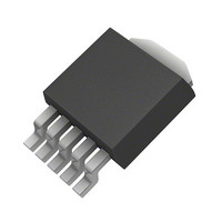
MIC35152WD TR Micrel Inc, MIC35152WD TR Datasheet - Page 6

MIC35152WD TR
Manufacturer Part Number
MIC35152WD TR
Description
IC REG LDO 1.5A ADJ TO-252-5
Manufacturer
Micrel Inc
Datasheet
1.MIC35152WD_TR.pdf
(8 pages)
Specifications of MIC35152WD TR
Regulator Topology
Positive Adjustable
Voltage - Output
1.24 ~ 5.4 V
Voltage - Input
2.25 ~ 6 V
Voltage - Dropout (typical)
0.365V @ 1.5A
Number Of Regulators
1
Current - Output
1.5A (Min)
Operating Temperature
-40°C ~ 125°C
Mounting Type
Surface Mount
Package / Case
DPak, TO-252 (5 leads + tab)
Lead Free Status / RoHS Status
Lead free / RoHS Compliant
Current - Limit (min)
-
Other names
576-3613-2
Application Information
The MIC35152 is a high-performance low-dropout
voltage regulator suitable for moderate to high-current
regulator applications. Its 600mV dropout voltage at full
load and over-temperature makes it especially valuable
in battery-powered systems and as high-efficiency noise
filters in post-regulator applications. Unlike older NPN-
pass transistor designs, there the minimum dropout
voltage is limited by the based-to-emitter voltage drop
and collector-to-emitter saturation voltage, dropout
performance of the PNP output of these devices is
limited only by the low V
A trade-off for the low dropout voltage is a varying base
drive requirement. Micrel’s Super ßeta PNP
reduces this drive requirement to only 2% to 5% of the
load current.
The MIC35152 regulator is fully protected from damage
due to fault conditions. Current limiting is provided. This
limiting is linear; output current during overload
conditions is constant. Thermal shutdown disables the
device when the die temperature exceeds the maximum
safe operating temperature. Transient protection allows
device (and load) survival even when the input voltage
spikes above and below nominal. The output structure of
these regulators allows voltages in excess of the desired
output voltage to be applied without reverse current flow.
Thermal Design
Linear regulators are simple to use. The most
complicated design parameters to consider are thermal
characteristics. Thermal design requires the following
application-specific parameters:
First, calculate the power dissipation of the regulator
from these numbers and the device parameters from this
datasheet.
Where the ground current is approximated by using
numbers from the “Electrical Characteristics” or “Typical
Characteristics.” Then, the heat sink thermal resistance
is determined with this formula:
Where T
2°C/W. The heat sink may be significantly reduced in
applications where the minimum input voltage is known
and is large compared with the dropout voltage. Use a
series input resistor to drop excessive voltage and
distribute the heat between this resistor and the
regulator. The low dropout properties of Micrel Super
ßeta PNP
Micrel, Inc.
October 2009
•
•
•
•
•
Maximum ambient temperature (T
Output current (I
Output voltage (V
Input voltage (V
Ground current (I
P
θ
SA
J(MAX)
D
=(V
®
=((T
regulators allow significant reductions in
IN
J(MAX)
≤ 125°C and θ
–V
OUT
–T
)I
OUT
A
IN
)/P
CE
OUT
GND
)
OUT
+V
saturation voltage.
D
)
)–(θ
)
)
IN
I
GND
JC
CS
+θ
is between 0°C and
CS
)
A
)
®
process
6
regulator power dissipation and the associated heat sink
without compromising performance. When this technique
is employed, a capacitor of at least 1.0µF is needed
directly between the input and regulator ground.
Refer to “Application Note 9” for further details and
examples on thermal design and heat sink applications.
With no heat sink in the application, calculate the
junction temperature to determine the maximum power
dissipation that will be allowed before exceeding the
maximum junction temperature of the MIC35152. The
maximum power allowed can be calculated using the
thermal resistance (θ
following criteria for the PCB design: 2 oz. copper and
100mm
As an example, given an expected maximum ambient
temperature (T
and I
Equation (1);
P
Next, calcualte the junction temperature for the expected
power dissipation.
T
Now determine the maximum power dissipation allowed
that would not exceed the IC’s maximum junction
temperature (125°C) without the use of a heat sink by
P
Output Capacitor
The MIC35152 requires an output capacitor for stable
operation. As a µCap LDO, the MIC35152 can operate
with ceramic output capacitors as long as the amount of
capacitance is 47µF or greater. For values of output
capacitance lower than 47µF, the recommended ESR
range is 200mΩ to 2Ω. The minimum value of output
capacitance recommended for the MIC35152 is 10µF.
For 47µF or greater, the ESR range recommended is
less than 1Ω. Ultra-low ESR ceramic capacitors are
recommended for output capacitance of 47µF or greater
to help improve transient response and noise reduction
at high frequency. X7R/X5R dielectric-type ceramic
capacitors
temperature performance. X7R-type capacitors change
capacitance by 15% over their operating temperature
range and are the most stable type of ceramic
capacitors. Z5U and Y5V dielectric capacitors change
value by as much as 50% and 60% respectively over
their operating temperature ranges. To use a ceramic
chip capacitor with Y5V dielectric, the value must be
much higher than an X7R ceramic capacitor to ensure
the same minimum capacitance over the equivalent
operating temperature range.
J
D
D(MAX)
=(θ
=(2.25V–1.75V)1.5A+(2.25V)(0.027A)=0.811W
OUT
JA
=(T
×P
2
copper area for the MIC35152.
= 1.5A, first calculate the expected P
J(MAX)
D
)+T
are
A
–T
A
=(56°C/W×0.811W)+75°C=120.4°C
) of 75°C with V
A
)/θ
recommended
JA
JA
=(125°C–75°C)/(56°C/W)=0.893W
) of the D-Pak adhering to the
IN
= 2.25V, V
because
M9999-102309-A
OUT
MIC35152
of
= 1.75V,
D
using
their


