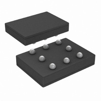
LP2967ITPX-2830/NOPB National Semiconductor, LP2967ITPX-2830/NOPB Datasheet - Page 6

LP2967ITPX-2830/NOPB
Manufacturer Part Number
LP2967ITPX-2830/NOPB
Description
IC VREG LDO DUAL 150MA 8USMD
Manufacturer
National Semiconductor
Datasheet
1.LP2967ITP-1833NOPB.pdf
(18 pages)
Specifications of LP2967ITPX-2830/NOPB
Regulator Topology
Positive Fixed
Voltage - Output
2.8V, 3V
Voltage - Input
2.1 ~ 16 V
Voltage - Dropout (typical)
0.24V @ 150mA
Number Of Regulators
2
Current - Output
150mA
Current - Limit (min)
200mA
Operating Temperature
-40°C ~ 125°C
Mounting Type
Surface Mount
Package / Case
8-MicroSMD
Number Of Outputs
2
Polarity
Positive
Input Voltage Max
16 V
Output Voltage
2.8 V, 3 V
Output Type
Fixed
Dropout Voltage (max)
0.01 V at 1 mA
Output Current
0.45 A (Typ), 0.45 A (Typ)
Line Regulation
0.08 %/V
Load Regulation
- 5 mV/V
Voltage Regulation Accuracy
+/- 1.25 %
Maximum Operating Temperature
+ 125 C
Mounting Style
SMD/SMT
Minimum Operating Temperature
- 40 C
Lead Free Status / RoHS Status
Lead free / RoHS Compliant
Other names
LP2967ITPX-2830
www.national.com
Electrical Characteristics
Note 1: Absolute maximum ratings indicate limits beyond which damage to the device may occur. Electrical specifications do not apply when operating the device
beyond its rated operating conditions.
Note 2: Rating is for the human body mode, a 100pF capacitor discharged through a 1.5kΩ resistor into each pin.
Note 3: The maximum allowable power dissipation is calculated by using P
ambient temperature, and θ
at elevated temperatures and is limited by T
Note 4: If used in a dual-supply system where the regulator load is returned to a negative supply, the LP2967 output must be diode-clamped to ground.
Note 5: The output PNP structure contains a diode between the V
will turn on this diode.
Note 6: Load regulation excursion over temperature is included in Output Voltage Tolerance.
Note 7: The dropout voltage of a regulator is defined as the minimum input-to-output differential required to stay within 100mV of the output voltage measured with
a 1V differential.
Limits in standard typeface are for T
range. Unless otherwise specified, V
Symbol
Xtalk
RR
Ripple Rejection
Crosstalk
Rejection
Parameter
JA
is the junction-to-ambient thermal resistance of the specified package. Therefore, the maximum power dissipation must be derated
JMAX
j
IN
= 25˚C, and limits in boldface type apply over the full operating junction temperature
, θ
C
V
square wave (trise and tfall =
100ns)
F = 120Hz
F = 800Hz
F = 1000Hz
F = 1600Hz
F = 10kHz
F = 100kHz
F = 1MHz
∆I
(15 mA/µs rise and fall slope)
I
∆V
∆I
(15 mA/µs rise and fall slope)
I
∆V
= V
LOAD
LOAD
JA
O(NOM)
BYPASS
LOAD
LOAD
OUT
OUT
and
O(NOM)
(Continued)
2 = 1mA
1 = 1mA
A
2/ ∆V
2/ ∆V
1 = 150 mA at 1kHz rate
2 = 150 mA at 1KHz rate
.
+ 1V + 100mV p-p
= 100nF, V
Conditions
+ 1V, I
IN
OUT
OUT
and V
1
1
L
OUT
= 1mA, C
DMAX
IN
terminals that is normally reverse-biased. Reversing the polarity from V
=
6
= (T
JMAX
IN
= 1µF,C
- T
A
/θ
JA
, where T
OUT
Min
= 4.7µF, V
JMAX
is the maximum junction temperature, T
−100
−100
Typ
−52
−54
−56
−58
−50
−47
−70
ON/OFF
= 1.6V.
Max
IN
and V
Units
A
dB
dB
is the
OUT


