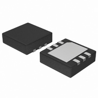
NCP623MN-50R2G ON Semiconductor, NCP623MN-50R2G Datasheet - Page 5

NCP623MN-50R2G
Manufacturer Part Number
NCP623MN-50R2G
Description
IC REG LDO 150MA 5.0V 6-DFN
Manufacturer
ON Semiconductor
Datasheet
1.NCP623MN-25R2G.pdf
(16 pages)
Specifications of NCP623MN-50R2G
Regulator Topology
Positive Fixed
Voltage - Output
5V
Voltage - Input
Up to 12V
Voltage - Dropout (typical)
0.18V @ 150mA
Number Of Regulators
1
Current - Output
150mA
Current - Limit (min)
175mA
Operating Temperature
-40°C ~ 85°C
Mounting Type
Surface Mount
Package / Case
6-VFDFN Exposed Pad
Lead Free Status / RoHS Status
Lead free / RoHS Compliant
Available stocks
Company
Part Number
Manufacturer
Quantity
Price
Company:
Part Number:
NCP623MN-50R2G
Manufacturer:
ON Semiconductor
Quantity:
2 300
change in load current at constant chip temperature.
the regulator output no longer maintains regulation against
further reductions in input voltage. Measured when the
output drops 100 mV below its nominal value (which is
measured at 1.0 V differential), dropout voltage is affected
by junction temperature, load current and minimum input
supply requirements.
output with a constant load and no input ripple, measured
over a specified frequency range.
dissipation for which the regulator will operate within
specifications.
regulator chip and is not delivered to the load.
change in the input voltage. The measurement is made under
conditions of low dissipation or by using pulse techniques
such that the average chip temperature is not significantly
affected.
undershoot response when input voltage is excited with a
given slope.
circuitry is provided to protect the integrated circuit in the
event that the maximum junction temperature is exceeded.
When activated, typically 150°C, the regulator turns off.
This feature is provided to prevent catastrophic failures from
accidental overheating.
Load Regulation − The change in output voltage for a
Dropout Voltage − The input/output differential at which
Output Noise Voltage − The RMS AC voltage at the
Maximum Power Dissipation − The maximum total
Quiescent Current − Current which is used to operate the
Line Regulation − The change in input voltage for a
Line Transient Response − Typical over− and
Thermal Protection − Internal thermal shutdown
http://onsemi.com
DEFINITIONS
5
package power dissipation is the power dissipation level at
which the junction temperature reaches its maximum value
i.e. 125°C. The junction temperature is rising while the
difference between the input power (V
output power (V
calculate the maximum power dissipation, maximum load
current or maximum input voltage (see Application Hints:
Protection).
is a lot increased when using appropriate application design.
Mounting pad configuration on the PCB, the board material
and also the ambient temperature are affected the rate of
temperature rise. It means that when the I
conductivity through PCB, the junction temperature will be
“low” even if the power dissipation is great.
evaluated by deliberately activating the thermal shutdown
of the circuit (by increasing the output current or raising the
input voltage for example).
subtracting the output power from the input power. All
variables are then well known: power dissipation, thermal
shutdown temperature (150°C for NCP623) and ambient
temperature.
Maximum Package Power Dissipation − The maximum
Depending on ambient temperature, it is possible to
The maximum power dissipation supported by the device
The thermal resistance of the whole circuit can be
Then you can calculate the power dissipation by
out
X I
out
) is increasing.
CC
C
has good thermal
X I
CC
) and the


