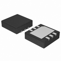
NCP623MN-50R2G ON Semiconductor, NCP623MN-50R2G Datasheet - Page 7

NCP623MN-50R2G
Manufacturer Part Number
NCP623MN-50R2G
Description
IC REG LDO 150MA 5.0V 6-DFN
Manufacturer
ON Semiconductor
Datasheet
1.NCP623MN-25R2G.pdf
(16 pages)
Specifications of NCP623MN-50R2G
Regulator Topology
Positive Fixed
Voltage - Output
5V
Voltage - Input
Up to 12V
Voltage - Dropout (typical)
0.18V @ 150mA
Number Of Regulators
1
Current - Output
150mA
Current - Limit (min)
175mA
Operating Temperature
-40°C ~ 85°C
Mounting Type
Surface Mount
Package / Case
6-VFDFN Exposed Pad
Lead Free Status / RoHS Status
Lead free / RoHS Compliant
Available stocks
Company
Part Number
Manufacturer
Quantity
Price
Company:
Part Number:
NCP623MN-50R2G
Manufacturer:
ON Semiconductor
Quantity:
2 300
applications, an immediate response to an enable signal is
vital. If noise is not a concern, the NCP623 without a bypass
capacitor settles in nearly 20 ms and typically delivers
65 mVRMS between 100 Hz and 100 kHz.
bypass capacitor to decrease the noise down to 25 mVRMS
between 100 Hz and 100 kHz. With the addition of the 10 nF
capacitor, the wake−up time expands up to 1.0 ms as shown
on the data−sheet curves. If an immediate response is
wanted, Figure 5 provides a solution to charge the bypass
Input
NCP623 Wake−up Improvement − In portable
In ultra low−noise systems, the designer needs a 10 nF
Bypass Pin when Enable Goes High (DFN6)
470 pF
On/Off
Figure 4. A PNP Transistor Drives the
+
220 k
C3
1.0 mF
C4
R2
MMBT2902LT1
6
1
Q1
NCP623
5
2
4
3
C1
10 nF
+
Output
http://onsemi.com
C2
1.0 mF
7
Output
capacitor with the enable signal without degrading the noise
response of the NCP623.
sends its wake−up signal by going high, the PNP base is
momentarily tied to ground. The PNP switch closes and
immediately charges the bypass capacitor C1 toward its
operating value. After a few ms, the PNP opens and becomes
totally transparent to the regulator.
which drops from 1.0 ms down to 30 ms. The value of C4
needs to be tweaked in order to avoid any bypass capacitor
overload during the wake−up transient.
At power−on, C4 is discharged. When the control logic
This circuit improves the response time of the regulator
Bypass Pin when Enable Goes High (Micro8)
+
Figure 5. A PNP Transistor Drives the
C2
1.0 mF
10 nF
C1
8
1
MMBT2902LT1
NCP623
7
2
6
3
Q1
4
5
R2
220 k
C4
470 pF
On/Off
+
C3
1.0 mF
Input


