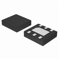
NCP565MN33T2G ON Semiconductor, NCP565MN33T2G Datasheet

NCP565MN33T2G
Specifications of NCP565MN33T2G
NCP565MN33T2GOSTR
Available stocks
Related parts for NCP565MN33T2G
NCP565MN33T2G Summary of contents
Page 1
NCP565/NCV565 1.5 A Low Dropout Linear Regulator The NCP565/NCV565 low dropout linear regulator will provide 1 fixed output voltage or an adjustable voltage down to 0.9 V. The fast loop response and low dropout voltage make this ...
Page 2
Vin Vin Vout NCP565 GND Cin Figure 1. Typical Application Schematic, Fixed Output PIN DESCRIPTION PAK 5 D PAK 3 Pin No. Pin No. Pin No. Adj. Version Fixed Version Adj. Version 1 − ...
Page 3
ABSOLUTE MAXIMUM RATINGS Input Voltage (Note 1) Output Pin Voltage Adjust Pin Voltage Stresses exceeding Maximum Ratings may damage the device. Maximum Ratings are stress ratings only. Functional operation above the Recommended Operating Conditions is not implied. Extended exposure to ...
Page 4
ELECTRICAL CHARACTERISTICS Characteristic ADJUSTABLE OUTPUT VERSION Reference Voltage (10 mA < I < 1 out Reference Voltage (10 mA < I < 1 out ADJ Pin Current (Note 5) Line Regulation ( mA) (Note ...
Page 5
0.9 V out(nom) 0.8975 0.8970 −50 − JUNCTION TEMPERATURE (°C) J Figure 5. Output Voltage vs. Temperature 3.80 3.70 3.60 3.50 ...
Page 6
F, FREQUENCY (Hz) Figure 11. Ripple Rejection vs. Frequency 10 0 −10 −20 −30 −40 1.50 1.00 0. 100 150 200 250 ...
Page 7
Start 1.0 kHz FREQUENCY (kHz) Figure 17. Noise Density vs. Frequency NOTE: Typical characteristics were measured with the same conditions as electrical characteristics. TYPICAL CHARACTERISTICS 100 ...
Page 8
APPLICATION INFORMATION The NCP565 low dropout linear regulator provides adjustable voltages at currents features ultra fast transient response and low dropout voltage. These devices contain output current limiting, short circuit protection and thermal shutdown protection. ...
Page 9
PCB Layout Considerations Good PCB layout plays an important role in achieving good load transient performance. Because it is very sensitive to its PCB layout, particular care has to be taken when tackling Printed Circuit Board (PCB) layout. The figures ...
Page 10
... Figure 22. Bottom Layer D1 VIN GND July, 2003 Figure 23. Silkscreen Layer http://onsemi.com 10 NCP565 ON Semiconductor www.onsemi.com VOUT GND ...
Page 11
... SMT Chip Resistor (0805) 15 SMT Chip Resistor (0805) 42 SMT Ceramic Capacitor (0603) 5 NCP565 Low Dropout Linear Regulator Designators Suppliers C1, C2, C3, C5 Sanyo Oscon C4 Sanyo Oscon R2 Vishay R1 Vishay C6 Vishay U1 ON Semiconductor http://onsemi.com 11 Part Number 16SA150M 10SL10M CRCW08051582F CRCW08054222F VJ0603A5R6KXAA NCP565D2TR4 ...
Page 12
Protection Diodes When large external capacitors are used with a linear regulator it is sometimes necessary to add protection diodes. If the input voltage of the regulator gets shorted, the output capacitor will discharge into the output of the regulator. ...
Page 13
... NCP565MN12T2G NCP565ST12T3G NCP565MN15T2G NCP565MN28T2G NCP565MN30T2G NCP565D2T33G NCP565D2T33R4G NCP565MN33T2G NCV565D2TG* NCV565D2TR4G* NCV565D2T12R4G* NCV565ST12T3G* †For information on tape and reel specifications, including part orientation and tape sizes, please refer to our Tape and Reel Packaging Specifications Brochure, BRD8011/D. *NCV prefix is for automotive and other applications requiring site and change controls. ...
Page 14
... OPTIONAL K A CHAMFER 0.010 (0.254 *For additional information on our Pb−Free strategy and soldering details, please download the ON Semiconductor Soldering and Mounting Techniques Reference Manual, SOLDERRM/D. PACKAGE DIMENSIONS 2 D PAK 3 D2T SUFFIX CASE 936−03 ISSUE C −T− TERMINAL SOLDERING FOOTPRINT* 10.49 8 ...
Page 15
... SOLDERING FOOTPRINT* 8.38 0.33 10.66 0.42 *For additional information on our Pb−Free strategy and soldering details, please download the ON Semiconductor Soldering and Mounting Techniques Reference Manual, SOLDERRM/D. PACKAGE DIMENSIONS 2 D PAK 5 CASE 936A−02 ISSUE C TERMINAL 6 NOTES: −T− 1. DIMENSIONING AND TOLERANCING PER ANSI Y14.5M, 1982. ...
Page 16
0.08 (0003) A1 2.0 0.079 PACKAGE DIMENSIONS SOT−223 (TO−261) CASE 318E−04 ISSUE N NOTES: 6. DIMENSIONING AND TOLERANCING PER ASME Y14.5M, 1994. 7. CONTROLLING DIMENSION: INCH. DIM ...
Page 17
... C *For additional information on our Pb−Free strategy and soldering details, please download the ON Semiconductor Soldering and Mounting Techniques Reference Manual, SOLDERRM/D. N. American Technical Support: 800−282−9855 Toll Free USA/Canada Europe, Middle East and Africa Technical Support: Phone: 421 33 790 2910 Japan Customer Focus Center Phone: 81− ...


