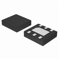
NCP565MN33T2G ON Semiconductor, NCP565MN33T2G Datasheet - Page 8

NCP565MN33T2G
Manufacturer Part Number
NCP565MN33T2G
Description
IC REG LDO 1.5A 3.3V 6-DFN
Manufacturer
ON Semiconductor
Datasheet
1.NCP565V12EVB.pdf
(17 pages)
Specifications of NCP565MN33T2G
Regulator Topology
Positive Fixed
Voltage - Output
3.3V
Voltage - Input
Up to 9V
Voltage - Dropout (typical)
0.9V @ 1.5A
Number Of Regulators
1
Current - Output
1.5A
Current - Limit (min)
1.6A
Operating Temperature
-40°C ~ 125°C
Mounting Type
Surface Mount
Package / Case
6-VSDFN Exposed Pad
Lead Free Status / RoHS Status
Lead free / RoHS Compliant
Other names
NCP565MN33T2G
NCP565MN33T2GOSTR
NCP565MN33T2GOSTR
Available stocks
Company
Part Number
Manufacturer
Quantity
Price
Company:
Part Number:
NCP565MN33T2G
Manufacturer:
ON Semiconductor
Quantity:
2 300
adjustable voltages at currents up to 1.5 A. It features ultra
fast transient response and low dropout voltage. These
devices contain output current limiting, short circuit
protection and thermal shutdown protection.
Input, Output Capacitor and Stability
transient response or if the regulator is located more than a
few inches from the power source. This will reduce the
circuit’s sensitivity to the input line impedance at high
frequencies and significantly enhance the output transient
response. Different types and different sizes of input
capacitors can be chosen dependent on the quality of power
supply. A 150 mF OSCON 16SA150M type from Sanyo
should be adequate for most applications. The bypass
capacitor should be mounted with shortest possible lead or
track length directly across the regulator’s input terminals.
remains stable with ceramic, tantalum, and aluminum−
electrolytic capacitors with a minimum value of 1.0 mF with
ESR between 50 mW and 2.5 W. The NCP565 is optimized
for use with a 150 mF OSCON 16SA150M type in parallel
with a 10 mF OSCON 10SL10M type from Sanyo. The
10 mF capacitor is used for best AC stability while 150 mF
capacitor is used for achieving excellent output transient
response. The output capacitors should be placed as close as
possible to the output pin of the device. If not, the excellent
load transient response of NCP565 will be degraded.
The NCP565 low dropout linear regulator provides
An input bypass capacitor is recommended to improve
The output capacitor is required for stability. The NCP565
APPLICATION INFORMATION
Pulse
Figure 19. Schematic for Transient Response Measurement
+
+
GEN
−V
GND
http://onsemi.com
V
CC
in
Scope Voltage Probe
Evaluation Board
8
NCP565
Adjustable Operation
regulators is shown in Figure 2. The adjustable device
develops and maintains the nominal 0.9 V reference voltage
between Adj and ground pins. A resistor divider network R1
and R2 causes a fixed current to flow to ground. This current
creates a voltage across R1 that adds to the 0.9 V across R2
and sets the overall output voltage.
normally much lower than the current flowing through R1
and R2, thus it generates a small output voltage error that can
usually be ignored.
Load Transient Measurement
microprocessor applications. Therefore good load transient
performance is required for the power stage. NCP565 has
the feature of ultra fast transient response. Its load transient
responses in Figures 13 through 16 are tested on evaluation
board shown in Figure 19. On the evaluation board, it
consists of NCP565 regulator circuit with decoupling and
filter capacitors and the pulse controlled current sink to
obtain load current transitions. The load current transitions
are measured by current probe. Because the signal from
current
un−synchronization between the load current transition and
output voltage response, which is shown in Figures 13
through 16.
The typical application circuit for the adjustable output
The output voltage is set according to the formula:
The adjust pin current, I
Large load current changes are always presented in
V out + V ref
probe
V
GND
out
has
V
R1 ) R2
some
R2
RL
Adj
time
, is typically 30 nA and
* I Adj
delay,
R2
it
causes


