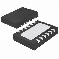
LT4356CDE-3#PBF Linear Technology, LT4356CDE-3#PBF Datasheet - Page 14

LT4356CDE-3#PBF
Manufacturer Part Number
LT4356CDE-3#PBF
Description
IC SURGE STOPPER W/LATCH 12-DFN
Manufacturer
Linear Technology
Datasheet
1.LT4356CS-3PBF.pdf
(24 pages)
Specifications of LT4356CDE-3#PBF
Voltage - Working
4 ~ 80V
Voltage - Clamping
27V Adj
Technology
Mixed Technology
Number Of Circuits
1
Applications
Automotive
Package / Case
12-DFN
Output Voltage
12V
Internal Switch
No
Supply Voltage Range
4V To 80V
Digital Ic Case Style
DFN
No. Of Pins
12
Operating Temperature Range
0°C To +70°C
Msl
MSL 1 - Unlimited
Termination Type
SMD
Rohs Compliant
Yes
Filter Terminals
SMD
Lead Free Status / RoHS Status
Lead free / RoHS Compliant
Power (watts)
-
Available stocks
Company
Part Number
Manufacturer
Quantity
Price
APPLICATIONS INFORMATION
LT4356-3
The LT4356-3 does not need extra compensation compo-
nents at the GATE pin for stability during an overvoltage or
overcurrent event. However, with fast, high voltage transient
steps at the input, a gate capacitor, C1, to ground is needed
to prevent turn-on of the N-channel MOSFET.
The extra gate capacitance slows down the turn off time
during fault conditions and may allow excessive current
during an output short event. An extra resistor, R1, in series
with the gate capacitor can improve the turn off time. A
diode, D1, should be placed across R1 with the cathode
connected to C1 as shown in Figure 5.
Auxiliary Amplifi er
An uncommitted amplifi er is included in the LT4356-3 to
provide fl exibility in the system design. With the negative
input connected internally to the 1.25V reference, the am-
plifi er can be connected as a level detect comparator with
external hysteresis. The open collector output pin, A
is capable of driving an opto or LED. It can also interface
with the system via a pull-up resistor to a supply voltage
up to 80V.
The amplifi er can also be confi gured as a low dropout
linear regulator controller. With an external PNP transistor,
such as 2N2905A, it can supply up to 100mA of current
with only a few hundred mV of dropout voltage. Current
limit can be easily included by adding two diodes and one
resistor (Figure 6). The amplifi er is turned off when the
LTC4356-3 is shut down.
14
R3
LT4356-3
GATE
Q1
Figure 5
IN4148W
43563 F05
D1
R1
C1
OUT
,
Reverse Input Protection
A blocking diode is commonly employed when reverse
input potential is possible, such as in automotive applica-
tions. This diode causes extra power loss, generates heat,
and reduces the available supply voltage range. During
cold crank, the extra voltage drop across the diode is
particularly undesirable.
The LT4356-3 is designed to withstand reverse voltage
without damage to itself or the load. The V
SHDN pins can withstand up to 60V of DC voltage below
the GND potential. Back-to-back MOSFETs must be used
to eliminate the current path through their body diodes
(Figure 7). Figure 8 shows the approach with a P-Channel
MOSFET in place of Q2.
INPUT
Figure 6. Auxiliary LDO Output with Optional Current Limit
Figure 7. Overvoltage Regulator with N-channel MOSFET
Reverse Input Protection
100k
SMAJ58CA
R6
12V
V
D2*
IN
*DIODES INC.
BAV99
D1*
LT4356DE-3
*4.7Ω
R
LIM
10mΩ
11
12
R
6
7
SNS
V
SHDN
A
IN
SNS
CC
OUT
+
2N2905A OR
5
1N4148
D1
BCP53
A
OUT
IN
11
2N3904
+
GND
Q3
12
IRLR2908
10
LT4356DE-3
R7
10k
Q2
R4
10Ω
R4
249k
R5
249k
TMR
43563 F06
1
R5
1M
C
0.1μF
IRLR2908
TMR
GATE
Q1
4
R3
10Ω
47nF
10μF
OUT
43563 F07
FLT
EN
FB
3
2
8
9
2.5V OUTPUT
≈ 150mA MAX
* OPTIONAL FOR
CC
V
I
CURRENT LIMIT
LIM
OUT
R1
59k
R2
4.99k
, SNS, and
≈
V
12V, 3A
CLAMPED
AT 16V
= 1.25
OUT
R
0.7
LIM
R4 + R5
43563fa
R5


