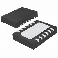
LT4356CDE-3#PBF Linear Technology, LT4356CDE-3#PBF Datasheet - Page 7

LT4356CDE-3#PBF
Manufacturer Part Number
LT4356CDE-3#PBF
Description
IC SURGE STOPPER W/LATCH 12-DFN
Manufacturer
Linear Technology
Datasheet
1.LT4356CS-3PBF.pdf
(24 pages)
Specifications of LT4356CDE-3#PBF
Voltage - Working
4 ~ 80V
Voltage - Clamping
27V Adj
Technology
Mixed Technology
Number Of Circuits
1
Applications
Automotive
Package / Case
12-DFN
Output Voltage
12V
Internal Switch
No
Supply Voltage Range
4V To 80V
Digital Ic Case Style
DFN
No. Of Pins
12
Operating Temperature Range
0°C To +70°C
Msl
MSL 1 - Unlimited
Termination Type
SMD
Rohs Compliant
Yes
Filter Terminals
SMD
Lead Free Status / RoHS Status
Lead free / RoHS Compliant
Power (watts)
-
Available stocks
Company
Part Number
Manufacturer
Quantity
Price
PIN FUNCTIONS
A
Open collector output of the auxiliary amplifi er. It is capable
of sinking up to 2mA from 80V. The negative input of the
amplifi er is internally connected to a 1.25V reference.
EN: Open-Collector Enable Output. The EN pin goes high
impedance when the voltage at the OUT pin is above (V
– 0.7V), indicating the external MOSFET is fully on. The
state of the pin is latched until the OUT pin voltage resets
at below 0.5V and goes back up above 2V. The internal
NPN is capable of sinking up to 3mA of current from 80V
to drive an LED or opto-coupler.
Exposed Pad: Exposed pad may be left open or connected
to device ground (GND).
FB: Voltage Regulator Feedback Input. Connect this pin
to the center tap of the output resistive divider connected
between the OUT pin and ground. During an overvoltage
condition, the GATE pin is servoed to maintain a 1.25V
threshold at the FB pin. This pin is clamped internally to
7V. Tie to GND to disable the OV clamp.
FLT: Open-Collector Fault Output. This pin pulls low
after the voltage at the TMR pin has reached the fault
threshold of 1.25V. It indicates the pass transistor is
about to turn off because either the supply voltage has
stayed at an elevated level for an extended period of
time (voltage fault) or the device is in an overcurrent
condition (current fault). The internal NPN is capable of
sinking up to 3mA of current from 80V to drive an LED or
opto-coupler.
GATE: N-Channel MOSFET Gate Drive Output. The GATE pin
is pulled up by an internal charge pump current source and
clamped to 14V above the OUT pin. Both voltage and cur-
rent amplifi ers control the GATE pin to regulate the output
voltage and limit the current through the MOSFET.
GND: Device Ground.
IN
Auxiliary Amplifi er. This amplifi er can be used as a level
detection comparator with external hysteresis or linear
regulator controlling an external PNP transistor. This pin is
clamped internally to 7V. Connect to ground if unused.
OUT
+
(DFN and SO Packages Only): Positive Input of the
(DFN and SO Packages Only): Amplifi er Output.
CC
OUT: Output Voltage Sense Input. This pin senses the
voltage at the source of the N-channel MOSFET and sets
the fault timer current. When the OUT pin voltage reaches
0.7V away from V
SHDN: Shutdown Control Input. The LT4356-3 can be
shut down to a low current mode by pulling the SHDN
pin below the shutdown threshold of 0.4V. All functions,
including the spare amplifi er, are turned off. Pull this pin
above 1.7V or disconnect it and allow the internal current
source to turn the part back on. After GATE pin pulls low
due to fault time out, the part can be restarted by pull-
ing the SHDN pin low for at least 100μs and pulled high
with a slew rate faster than 10V/ms. The leakage current
to ground at the pin should be limited to no more than
1μA if no pull up device is used to turn the part on. The
SHDN pin can be pulled up to 100V or below GND by 60V
without damage.
SNS: Current Sense Input. Connect this pin to the output of
the current sense resistor. The current limit circuit controls
the GATE pin to limit the sense voltage between V
SNS pins to 50mV. At the same time the sense amplifi er
also starts a current source to charge up the TMR pin.
This pin can be pulled below GND by up to 60V, though
the voltage difference with the V
less than 30V. Connect to V
TMR: Fault Timer Input. Connect a capacitor between this
pin and ground to set the times for early warning and fault
periods. The current charging up this pin during fault
conditions depends on the voltage difference between the
V
pulls low to indicate the detection of a fault condition. If
the condition persists, the pass transistor turns off when
V
low even after the fault condition has disappeared and the
voltage at the TMR pin has reached 0.5V.
V
input ranges from 4V to 80V for normal operation. It
can also be pulled below ground potential by up to 60V
during a reverse battery condition, without damaging the
part. The supply current is reduced to 7μA with all the
functional blocks off.
TMR
CC
CC
: Positive Supply Voltage Input. The positive supply
and OUT pins. When V
reaches the threshold of 1.35V. The GATE pin remains
CC
, the EN pin goes high impedance.
TMR
CC
if unused.
reaches 1.25V, the FLT pin
CC
pin must be limited to
LT4356-3
CC
43563fa
7
and


