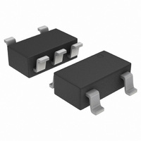
NCP360SNAET1G ON Semiconductor, NCP360SNAET1G Datasheet

NCP360SNAET1G
Specifications of NCP360SNAET1G
NCP360SNAET1GOSTR
Available stocks
Related parts for NCP360SNAET1G
NCP360SNAET1G Summary of contents
Page 1
NCP360 USB Positive Overvoltage Protection Controller with Internal PMOS FET and Status FLAG The NCP360 disconnects systems at its output when wrong VBUS operating conditions are detected at its input. The system is positive overvoltage protected up to +20 V. ...
Page 2
EN 1 GND 2 PAD1 IN 3 UDFN6 PIN FUNCTION DESCRIPTION (UDFN6 Package) Pin No. Name Type 1 EN INPUT Enable Pin. The device enters in shutdown mode when this pin is tied to a high level. In this case ...
Page 3
INPUT X5R 0603 C1 Figure 1. Typical Application Circuit (UDFN Pinout) INPUT EN LDO OUTPUT 3 4 OUT IN 5 OUT X5R 0603 NCP360 FLAG FLAG GND 2 ...
Page 4
MAXIMUM RATINGS Rating Minimum Voltage (IN to GND) Minimum Voltage (All others to GND) Maximum Voltage (IN to GND) Maximum Voltage (All others to GND) Maximum Current from Vin to Vout (PMOS) (Note 1) Thermal Resistance, Junction−to−Air (Note 2) Operating ...
Page 5
ELECTRICAL CHARACTERISTICS (Min/Max limits values (−40°C < T < +85°C) and V A Characteristic Symbol Input Voltage Range Undervoltage Lockout Threshold UVLO Undervoltage Lockout UVLO Hysteresis Overvoltage Lockout Threshold OVLO Overvoltage Lockout Hysteresis OVLO V versus V Dopout V in ...
Page 6
UVLO V > out t start FLAG 1.2 V Figure 3. Start Up Sequence EN 1 dis V out 0 − DS(on) FLAG Figure ...
Page 7
TYPICAL OPERATING CHARACTERISTICS Figure 9. Startup V = Ch1 Ch3 in out Figure 11. Output Turn Off Time V = Ch1 Ch2 in out Figure 13. Disable Time EN = Ch1 Ch2, FLAG = ...
Page 8
TYPICAL OPERATING CHARACTERISTICS Figure 15. Direct Output Short Circuit 180 160 140 120 100 80 25° Figure 17. Supply Quiescent Current vs. V 450 400 350 300 250 200 150 100 50 0 −50 ...
Page 9
In Operation NCP360 provides overvoltage protection for positive voltage PMOS FET protects the systems (i.e.: VBUS) connected on the V out over−voltage. The Output follows the VBUS level until OVLO threshold is overtaken. Undervoltage Lockout ...
Page 10
In every case, we recommend to make thermal measurement on final application board to make sure of the final Thermal Resistance. 380 330 280 230 180 130 80 0 100 Figure 20. Thermal Resistance of UDFN 2x2 and TSOP Packages ...
Page 11
... ORDERING INFORMATION Device NCP360MUTBG NCP360MUTXG NCP360SNT1G NCP360SNAET1G NCP360SNAFT1G NCP360SNAIT1G †For information on tape and reel specifications, including part orientation and tape sizes, please refer to our Tape and Reel Packaging Specifications Brochure, BRD8011/D. SELECTION GUIDE The NCP360 can be available in several undervoltage and overvoltage thresholds versions. Part number is designated as follows: ...
Page 12
... SOLDERING FOOTPRINT* A 0.95 C SEATING PLANE *For additional information on our Pb−Free strategy and soldering 0. details, please download the ON Semiconductor Soldering and 0.05 C Mounting Techniques Reference Manual, SOLDERRM/D. http://onsemi.com 12 ASME Y14.5M, 1994. PAD AS WELL AS THE TERMINALS. MILLIMETERS DIM MIN MAX A 0.45 0.55 A1 ...
Page 13
... H T *For additional information on our Pb−Free strategy and soldering details, please download the ON Semiconductor Soldering and Mounting Techniques Reference Manual, SOLDERRM/D. ON Semiconductor and are registered trademarks of Semiconductor Components Industries, LLC (SCILLC). SCILLC reserves the right to make changes without further notice to any products herein. SCILLC makes no warranty, representation or guarantee regarding the suitability of its products for any particular purpose, nor does SCILLC assume any liability arising out of the application or use of any product or circuit, and specifically disclaims any and all liability, including without limitation special, consequential or incidental damages. “ ...


