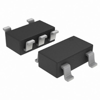
NCP360SNAET1G ON Semiconductor, NCP360SNAET1G Datasheet - Page 9

NCP360SNAET1G
Manufacturer Part Number
NCP360SNAET1G
Description
IC CTLR USB POS OVP FET SOT23-5
Manufacturer
ON Semiconductor
Type
Power Supply Controllerr
Datasheet
1.NCP360SNAET1G.pdf
(13 pages)
Specifications of NCP360SNAET1G
Voltage - Working
1.2 ~ 20V
Voltage - Clamping
7.4V
Technology
Mixed Technology
Number Of Circuits
1
Applications
USB
Package / Case
TSOT-23-5, TSOT-5, TSOP-5
Number Of Voltages Monitored
1
Monitored Voltage
1.2 V to 20 V
Manual Reset
No
Watchdog
No
Supply Voltage (max)
20 V
Supply Voltage (min)
1.2 V
Mounting Style
SMD/SMT
Maximum Operating Temperature
+ 85 C
Minimum Operating Temperature
- 40 C
Lead Free Status / RoHS Status
Lead free / RoHS Compliant
Power (watts)
-
Lead Free Status / Rohs Status
Lead free / RoHS Compliant
Other names
NCP360SNAET1G
NCP360SNAET1GOSTR
NCP360SNAET1GOSTR
Available stocks
Company
Part Number
Manufacturer
Quantity
Price
Company:
Part Number:
NCP360SNAET1G
Manufacturer:
AAT
Quantity:
4 600
Company:
Part Number:
NCP360SNAET1G
Manufacturer:
ON
Quantity:
3 000
Part Number:
NCP360SNAET1G
Manufacturer:
ON/安森美
Quantity:
20 000
In Operation
voltage, up to 20 V. A PMOS FET protects the systems
(i.e.: VBUS) connected on the V
over−voltage. The Output follows the VBUS level until
OVLO threshold is overtaken.
Undervoltage Lockout (UVLO)
device has a built−in undervoltage lock out (UVLO)
circuit. During V
disconnected from input until V
nominal. The FLAGV output is pulled to low as long as V
does not reach UVLO threshold. This circuit has a UVLO
hysteresis to provide noise immunity to transient condition.
Overvoltage Lockout (OVLO)
overvoltage, the device has a built−in overvoltage lock out
(OVLO) circuit. During overvoltage condition, the output
remains disabled until the input voltage exceeds OVLO −
Hysteresis.
OVLO. This circuit has a OVLO hysteresis to provide noise
immunity to transient
FLAG Output
systems that a fault has occurred.
exceeded When V
FLAG is held high. The pin is an open drain output, thus a
pull up resistor (typically 1 MW− Minimum 10 kW) must
be provided to V
EN Input
to low or connected to ground. A high level on the pin
disconnects OUT pin from IN pin. EN does not overdrive
an OVLO or UVLO fault.
V
NCP360 provides overvoltage protection for positive
To ensure proper operation under any conditions, the
OVLO
UVLO
OVLO
UVLO
To protect connected systems on V
FLAG output is tied to low until V
NCP360 provides a FLAG output, which alerts external
This pin is tied to low as soon the OVLO threshold is
To enable normal operation, the EN pin shall be forced
in
20 V
V
(V)
out
0
0
Figure 18. Output Characteristic vs. V
in
battery
positive going slope, the output remains
in
. FLAG pin is an open drain output.
conditions.
level recovers normal condition,
in
out
voltage is above 3.2 V
pin, against positive
in
is higher than
out
in
pin from
http://onsemi.com
in
9
Internal PMOS FET
systems,
overvoltage. Regarding electrical characteristics, the
R
V
Figure 16).
ESD Tests
pin, 1 mF mounted on board).
protected input. In Contact condition, V
protected input.
electrostatic discharge waveform.
PCB Recommendations
the PCB rules must be respected to properly evacuate the
heat out of the silicon. The UDFN PAD1 must be connected
to ground plane to increase the heat transfer if necessary
from an application standpoint. Of course, in any case, this
pad shall be not connected to any other potential.
decreased, allowing higher charge current to fill the battery.
between package and silicon) can handle up to 1 A (higher
than thermal capability), the following calculation shows
two different example of current capability, depending on
PCB area:
•
•
DSon
out
NCP360 includes an internal PMOS FET to protect the
NCP360 fully support the IEC61000−4−2, level 4 (Input
That means, in Air condition, V
Please refer to Fig 19 to see the IEC 61000−4−2
The NCP360 integrates a 500 mA rated PMOS FET, and
By increasing PCB area, the R
Taking into account that internal bondings (wires
I = √(T
I = 625 mA
With 305°C/W (without PCB area), allowing DC
current is 500 mA
With 260°C/W (200 mm
allows with a 85°C ambient temperature is:
pin, characterized by V
, during normal operation, will create low losses on
J
-T
connected on OUT pin, from positive
A
)/(R
qJA
x R
Figure 19.
DSON
2
), the charge DC current
in
)
versus V
qJA
in
of the package can be
has a ±15 kV ESD
in
out
has ±8 kV ESD
dropout. (See


