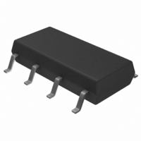
TISP61089BDR Bourns Inc., TISP61089BDR Datasheet - Page 9

TISP61089BDR
Manufacturer Part Number
TISP61089BDR
Description
SURGE SUPP SLIC PROG HV 8-SOP
Manufacturer
Bourns Inc.
Datasheet
1.TISP61089BDR-S.pdf
(20 pages)
Specifications of TISP61089BDR
Package / Case
8-SOIC (3.9mm Width)
Voltage - Breakover
*
Voltage - Off State
170V
Current - Peak Pulse (10 X 1000µs)
30A
Current - Hold (ih)
150mA
Number Of Elements
2
Capacitance
100pF
Applications
SLIC
Number Of Circuits
2
Voltage - Working
-100V
Voltage - Clamping
-112V
Technology
Mixed Technology
Breakover Current Ibo Max
6.5 A
Rated Repetitive Off-state Voltage Vdrm
170 V
Off-state Leakage Current @ Vdrm Idrm
0.005 mA
Holding Current (ih Max)
150 mA
Mounting Style
SMD/SMT
Power (watts)
-
Lead Free Status / RoHS Status
Lead free / RoHS Compliant
Available stocks
Company
Part Number
Manufacturer
Quantity
Price
Part Number:
TISP61089BDR
Manufacturer:
BOURNS/伯恩斯
Quantity:
20 000
Company:
Part Number:
TISP61089BDR-S
Manufacturer:
LITTLEFUSE
Quantity:
4 114
Company:
Part Number:
TISP61089BDR-S
Manufacturer:
Bourns Inc.
Quantity:
31 562
Part Number:
TISP61089BDR-S
Manufacturer:
BOURNS/伯恩斯
Quantity:
20 000
protection voltage, the length of the capacitor to gate terminal tracking should be minimized. Inductive voltages in the protector cathode wiring
will also increase the protection voltage. These voltages can be minimized by routing the SLIC connection through the protector as shown in
Figure 6.
Figure 9, which has a 10 A/µs rate of impulse current rise, shows a positive gate charge (Q
decoupling capacitor used, the increase in gate supply is about 1 V (= Q
But, the voltage increase does not directly add to the protection voltage as the supply voltage change reaches a maximum at 0.4 µs, when the
gate current reverses polarity, and the protection voltage peaks earlier at 0.3 µs. In Figure 9, the peak clamping voltage (V
increase of 5.5 V on the nominal gate supply voltage. This 5.5 V increase is the sum of the supply rail increase at that time, (0.5 V), and the
protection circuit’s cathode diode to supply rail breakover voltage (5 V). In practice, use of the recommended 220 nF gate decoupling capacitor
would give a supply rail increase of about 0.3 V and a V
Voltage Stress Levels on the TISP61089B
Figure 10 shows the protector electrodes. The package terminal designated gate, G, is the transistor base, B, electrode connection and so is
marked as B (G). The following junctions are subject to voltage stress: Transistor EB and CB, SCR AK (off state) and the antiparallel diode
(reverse blocking). This clause covers the necessary testing to ensure the junctions are good.
Testing transistor CB and EB: The maximum voltage stress level for the TISP61089B is V
diode voltage overshoot, V
the common (0 V) for this test (see Figure 10). The measured current, I
Gated Protectors (Continued)
TISP61089B High Voltage Ringing SLIC Protector
FRM
Figure 9. Protector Fast Impulse Clamping and Switching Waveforms
. The current flowing out of the G terminal is measured at V
-20
-40
-60
-80
-1
-2
-3
-4
-5
0
1
0
0.0
0.0
Q GS
(BO)
value of about -77.3 V.
V K
0.5
0.5
Time - µs
Time - µs
GKS
GS
I G
, is the sum of the junction currents I
/C1). This change is just visible on the -72 V gate voltage, V
Customers should verify actual device performance in their specific applications.
1.0
1.0
BATH
BATH
GS
V BATH
) of about 0.1 µC. With the 0.1 µF gate
I K
with the addition of the short term antiparallel
plus V
AI6XDE
1.5
FRM
1.5
Specifications are subject to change without notice.
. The SCR K terminal is shorted to
CB
and I
OCTOBER 2000 - REVISED JULY 2008
EB
(BO)
.
) is -77.5 V, an
BATH
.


