DLP-USB1232H DLP Design Inc, DLP-USB1232H Datasheet - Page 8
DLP-USB1232H
Manufacturer Part Number
DLP-USB1232H
Description
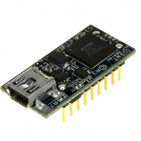
MODULE USB-TO-UART/FIFO HS 18DIP
Manufacturer
DLP Design Inc
Datasheet
1.DLP-USB1232H.pdf
(14 pages)
Specifications of DLP-USB1232H
Convert From (adapter End)
USB
Convert To (adapter End)
UART/FIFO
Features
2.0 High Speed USB
Interface Type
USB
Data Bus Width
8 bit
Operating Supply Voltage
4 V to 5.5 V
For Use With/related Products
Windows® Vista, 2000, XP, Mac
Lead Free Status / RoHS Status
Lead free / RoHS Compliant
Lead Free Status / RoHS Status
Lead free / RoHS Compliant, Lead free / RoHS Compliant
Other names
813-1026


Rev. 1.3 (December 2009)
P
P
I
10
11
12
13
14
15
16
17
18
I
N
N
1
2
3
4
5
6
7
8
9
#
#
P
GROUND
DB2 - FIFO Data Bus Bit 2
DB7 - FIFO Data Bus Bit 7
DB5 - FIFO Data Bus Bit 5
DB3 - FIFO Data Bus Bit 3
PWREN -
SIWUA -The Send Immediate / WakeUp signal combines two functions on a single pin. If
USB is in suspend mode (PWREN# = 1) and remote wakeup is enabled in the EEPROM,
strobing this pin low will cause the device to request a resume on the USB Bus.
Normally, this can be used to wake up the Host PC. During normal operation (PWREN#
= 0), if this pin is strobed low any data in the device TX buffer will be sent out over USB
on the next Bulk-IN request from the drivers regardless of the pending packet size.
This can be used to optimize USB transfer speed for some applications. Tie this pin to
VCCIO if not used.
EXTVCC - Use for applying main power (4.5 to 5.25 volts) to the module. Connect to
PORTVCC (Pin 9) if the module is to be powered by the USB port (typical configuration).
PORTVCC - Power from the USB port. Connect to EXTVCC (Pin 8) if the module is to
be powered by the USB port (typical configuration). 500mA is the maximum current
available to the USB adapter and target electronics if the USB device is configured for
high power.
GROUND
RD# - When pulled low, RD# takes the 8 data lines from a high-impedance state to the
current byte in the FIFO’s buffer. Taking RD# high returns the data pins to a high-
impedance state and prepares the next byte (if available) in the FIFO to be read.
WR - When taken from a high to a low state, WR reads the 8 data lines and writes the
byte into the FIFO’s transmit buffer. Data written to the transmit buffer is sent to the host
PC within the TX buffer timeout value (default 16mS) and placed in the buffer that was
created when the USB port was opened. The FT245R allows the TX buffer timeout value
to be reprogrammed to a value between 1 and 255mS.
DB6 - FIFO Data Bus Bit 6
TXE# - When high, do not write data into the FIFO. When low, data can be written into
the FIFO by strobing WR high, then low. During reset this signal pin is tri-state. Data is
latched into the FIFO on the falling edge of the WR pin.
RXF# - When low, at least 1 byte is present in the FIFO’s receive buffer and is ready to
be read with RD#. RXF# goes high when the receive buffer is empty. During reset this
signal pin is tri-state. If the Remote Wakeup option is enabled in the internal EEPROM,
during USB Suspend Mode (PWREN#=1) RXF# becomes an input. This can be used to
wake up the USB host from Suspend Mode by strobing this pin low for a minimum of
20ms which will cause the device to request a resume on the USB bus.
DB1 - FIFO Data Bus Bit 1
DB4 - FIFO Data Bus Bit 4
DB0 - FIFO Data Bus Bit 0
P
A
A
R
R
A
A
L
L
L
L
E
E
PWREN# = 0: Normal operation.
PWREN# = 1: USB SUSPEND mode or device has not been configured.
This can be used by external circuitry to power down logic when device is in USB
suspend or has not been configured.
Active low power-enable output.
L
L
S
S
I
I
G
G
N
N
A
A
L
L
U
U
S
S
A
A
G
G
E
E
D
D
E
E
S
S
C
C
R
R
I
I
P
P
8
T
T
I
I
O
O
N
N
© DLP Design, Inc.
Related parts for DLP-USB1232H
Image
Part Number
Description
Manufacturer
Datasheet
Request
R

Part Number:
Description:
Interface Modules & Development Tools Legacy USB Adapter
Manufacturer:
DLP Design Inc
Datasheet:

Part Number:
Description:
MODULE USB ADAPTER FOR FT2232D
Manufacturer:
DLP Design Inc
Datasheet:

Part Number:
Description:
MODULE USB-TO-FPGA TOOL W/MANUAL
Manufacturer:
DLP Design Inc
Datasheet:

Part Number:
Description:
Interface Modules & Development Tools RETRACTABLE USB CBL USB TO MINI USB
Manufacturer:
DLP Design Inc
Part Number:
Description:
Interface Modules & Development Tools USB FPGA Module w/ Xilinx XC3S400A
Manufacturer:
DLP Design Inc
Datasheet:

Part Number:
Description:
MODULE USB-TO-PARL FIFO 18-DIP
Manufacturer:
DLP Design Inc
Datasheet:

Part Number:
Description:
MODULE USB-TO-SRL UART 18-DIP
Manufacturer:
DLP Design Inc
Datasheet:

Part Number:
Description:
MODULE USB ADAPTR FOR FT2232D LP
Manufacturer:
DLP Design Inc
Datasheet:

Part Number:
Description:
MODULE USB-MCU FT245RL W/16F877A
Manufacturer:
DLP Design Inc
Datasheet:

Part Number:
Description:
MODULE USB-TO-FPGA TRAINING TOOL
Manufacturer:
DLP Design Inc
Datasheet:

Part Number:
Description:
MODULE USB-MCU FT232R W/18F2410
Manufacturer:
DLP Design Inc
Datasheet:

Part Number:
Description:
MODULE USB-MCU FT245RL W/SX48
Manufacturer:
DLP Design Inc
Datasheet:

Part Number:
Description:
MODULE USB-MCU FT2232D W/16F877A
Manufacturer:
DLP Design Inc
Datasheet:

Part Number:
Description:
MODULE USB-TO-FPGA SPARTAN3
Manufacturer:
DLP Design Inc
Datasheet:

Part Number:
Description:
MOD USB-MCU FT245RL W/18LF8722
Manufacturer:
DLP Design Inc
Datasheet: