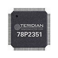
78P2351-IGT/F Maxim Integrated Products, 78P2351-IGT/F Datasheet - Page 13

78P2351-IGT/F
Manufacturer Part Number
78P2351-IGT/F
Description
LINE INTERFACE UNIT 100-LQFP
Manufacturer
Maxim Integrated Products
Specifications of 78P2351-IGT/F
Number Of Channels Per Chip
1
Propagation Delay Time
10 ns
Supply Voltage (max)
3.45 V
Supply Voltage (min)
3.15 V
Maximum Operating Temperature
+ 85 C
Package / Case
LQFP-100
Minimum Operating Temperature
- 40 C
Mounting Style
SMD/SMT
Lead Free Status / RoHS Status
Lead free / RoHS Compliant
Available stocks
Company
Part Number
Manufacturer
Quantity
Price
Company:
Part Number:
78P2351-IGT/F
Manufacturer:
VISHAY
Quantity:
14 105
Company:
Part Number:
78P2351-IGT/F
Manufacturer:
MAXIM
Quantity:
4
Company:
Part Number:
78P2351-IGT/F
Manufacturer:
Maxim Integrated
Quantity:
10 000
REGISTER DESCRIPTION
PORT-SPECIFIC REGISTERS
For PA[3:0] = 1 only. Accessing a register with port address greater than 1 constitutes an invalid command.
ADDRESS 1-0: MODE CONTROL REGISTER
Page: 13 of 42
BIT
1:0
7
6
5
4
3
2
SMOD[1]
SMOD[0]
PMODE
NAME
PDRX
PDTX
MON
--
TYPE
R/W
R/W
R/W
R/W
R/W
R/W
R/W
VALUE
DFLT
00
X
X
X
0
0
0
(continued)
DESCRIPTION
Transmitter Power-Down:
Receiver Power-Down:
Parallel Mode Interface Selection:
Serial Mode Interface Selection:
Receive Monitor Mode Enable:
NOTE: Monitor mode is only available in CMI mode.
Reserved
When PAR=0, PMODE is invalid and defaults to logic ‘1’;
When PAR=1, (Master Control Register: bit 5), PMODE selects the
source of the transmit parallel clock, either taken from the framer
externally or generated internally. Default value is determined by
CKMODE pin setting upon power up or reset.
When PAR=0 (Master Control Register: bit 5), SMOD[1:0] configures
the transmitter’s system interface.
CKMODE pin setting upon power up or reset.
SMOD[1] SMOD[0]
When PAR=1 (Master Control Register: bit 5), setting SMOD[1:0] = 11
will enable Loop Timing Mode.
CKMODE pin setting upon power up or reset as follows:
2006 Teridian Semiconductor Corporation
0
1
0
1
0 : Normal Operation
1 : Power-Down. CMI Transmit output is tri-stated.
0 : Normal Operation
1 : Power-Down
0: Normal Operation
1: Adds 20dB of flat gain to the receive signal before equalization.
0: Slave Timing. PICK clock input to the transmitter
1: Master Timing. PTOCK clock output from the transmitter
CKMODE Low
CKMODE Float
CKMODE High
0
0
1
1
Synchronous clock and data are passed through a
FIFO. The CDR is bypassed.
Synchronous data is passed through the CDR and
then through the FIFO.
Plesiochronous data is passed through the CDR to
recover a clock. FIFO is bypassed because the
data is not synchronous with the reference clock.
Loop Timing Mode Enable: The recovered receive
clock is used as the reference for the transmit DLL
and FIFO.
SMOD[1:0] default = 00 (no effect)
SMOD[1:0] default = 11 (loop-timing enable)
SMOD[1:0] default = 01 (no effect)
Default values are determined by
Default values determined by
OC-3/ STM1-E/ E4 LIU
Single Channel
78P2351
Rev. 2.4


