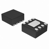
NCP5359AMNR2G ON Semiconductor, NCP5359AMNR2G Datasheet - Page 3

NCP5359AMNR2G
Manufacturer Part Number
NCP5359AMNR2G
Description
IC MOSFET GATE DVR DUAL 8-DFN
Manufacturer
ON Semiconductor
Type
High Side/Low Sider
Datasheet
1.NCP5359AMNTBG.pdf
(9 pages)
Specifications of NCP5359AMNR2G
Configuration
High and Low Side, Synchronous
Input Type
PWM
Delay Time
10.0ns
Number Of Configurations
1
Number Of Outputs
2
High Side Voltage - Max (bootstrap)
30V
Voltage - Supply
10 V ~ 13.2 V
Operating Temperature
0°C ~ 85°C
Mounting Type
Surface Mount
Package / Case
8-VFDFN Exposed Pad
Product
MOSFET Gate Drivers
Propagation Delay Time
25 ns
Supply Voltage (max)
15 V
Supply Voltage (min)
- 0.3 V
Maximum Operating Temperature
+ 150 C
Mounting Style
SMD/SMT
Minimum Operating Temperature
0 C
Output Voltage
35 V
Lead Free Status / RoHS Status
Lead free / RoHS Compliant
Current - Peak
-
Lead Free Status / Rohs Status
Lead free / RoHS Compliant
Available stocks
Company
Part Number
Manufacturer
Quantity
Price
Company:
Part Number:
NCP5359AMNR2G
Manufacturer:
FREESCALE
Quantity:
101
Part Number:
NCP5359AMNR2G
Manufacturer:
ON/安森美
Quantity:
20 000
PIN DESCRIPTION
10 V to 13.2 V
SOIC−8
1
2
3
4
5
6
7
8
PWM
EN
DFN8
1
2
3
4
5
6
7
8
Symbol
DRVH
DRVL
PWM
VCC
GND
BST
SW
EN
Upper MOSFET Floating Bootstrap Supply Pin
PWM Input Pin
When PWM voltage is higher than 2.2 V, DRVH will set to 1 and DRVL set to 0
When PWM voltage is lower than 0.8 V, DRVL will set to 1 and DRVH set to 0
When 0.8 V < PWM < 2.2 V and SW < 0, DRVL will set to 1
When 0.8 V < PWM < 2.2 V and SW > 0, DRVL will set to 0
Enable Pin
When OVP, TSD or UVLO has happened, the gate driver will pull the pin to low
Connect to Input Power Supply 10 V to 13.2 V
Low Side Gate Drive Output
Ground Pin
Switch Node Pin
High Side Gate Drive Output
BST
PWM
EN
VCC
Figure 2. Typical Application
DRVH
DRVL
GND
http://onsemi.com
SW
3
Description
4 V to 15 V
VOUT


