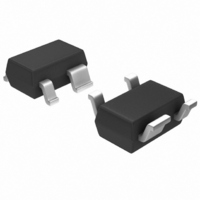
MGA-72543-TR1G Avago Technologies US Inc., MGA-72543-TR1G Datasheet - Page 13

MGA-72543-TR1G
Manufacturer Part Number
MGA-72543-TR1G
Description
IC AMP MMIC LNA GAAS 3V SOT-343
Manufacturer
Avago Technologies US Inc.
Type
General Purpose Amplifierr
Datasheet
1.MGA-72543-TR1G.pdf
(21 pages)
Specifications of MGA-72543-TR1G
Noise Figure
1.42dB
Package / Case
SC-70-4, SC-82-4, SOT-323-4, SOT-343
Current - Supply
60mA ~ 70mA
Frequency
100MHz ~ 6GHz
Gain
13.6dB
P1db
3.2dBm ~ 17.1dBm @ 5mA ~ 60mA
Rf Type
CDMA, TDMA
Test Frequency
2GHz
Voltage - Supply
2.7V ~ 4.2V
Mounting Style
SMD/SMT
Technology
Low Noise Amplifier
Number Of Channels
1
Operating Frequency
6000 MHz
Operating Supply Voltage
3 V
Supply Current
60 mA
Maximum Power Dissipation
250 mW
Maximum Operating Temperature
+ 150 C
Manufacturer's Type
Low Noise Amplifier
Frequency (max)
6GHz
Operating Supply Voltage (min)
2.7V
Operating Supply Voltage (typ)
3V
Operating Supply Voltage (max)
4.2V
Package Type
SOT-343
Mounting
Surface Mount
Pin Count
3 +Tab
Noise Figure (typ)
1.7@6000MHzdB
Lead Free Status / RoHS Status
Lead free / RoHS Compliant
Lead Free Status / RoHS Status
Lead free / RoHS Compliant, Lead free / RoHS Compliant
Other names
516-1829-2
MGA-72543-TR1G
MGA-72543-TR1G
Available stocks
Company
Part Number
Manufacturer
Quantity
Price
Company:
Part Number:
MGA-72543-TR1G
Manufacturer:
AVAGO
Quantity:
201
Company:
Part Number:
MGA-72543-TR1G
Manufacturer:
AVAGO
Quantity:
55 000
Part Number:
MGA-72543-TR1G
Manufacturer:
AVAGO/安华高
Quantity:
20 000
Applications Information: Designing with the
MGA-72543 RFIC Amplifier/Bypass Switch
Description
The MGA-72543 is a single-stage, GaAs RFIC amplifier
with an
integrated bypass switch. A functional diagram of the
MGA-72543 is shown in Figure 1.
The MGA-72543 is designed for receivers and transmitters
operating from 100 MHz to 6 GHz with an emphasis on
1.9 GHz CDMA applications. The MGA-72543 combines
low noise performance with high linearity to make it
especially advantageous for use in receiver front-ends.
Figure 1. MGA-72543 Functional Diagram.
The purpose of the switch feature is to prevent distortion
of high signal levels in receiver applications by bypass-
ing the amplifier altogether. The bypass switch can be
thought of as a 1-bit digital AGC circuit that not only pre-
vents distortion by bypassing the MGA-72543 amplifier,
but also reduces front-end system gain by approximately
16 dB to avoid overdriving subsequent stages in the re-
ceiver such as the mixer.
An additional feature of the MGA-72543 is the ability to
externally set device current to balance output power
capability and high linearity with low DC power consump-
tion. The adjustable current feature of the MGA-72543
allows it to deliver output power levels in excess of +15
dBm (P1dB), thus extending its use to other system ap-
plications such as transmitter driver stages.
The MGA-72543 is designed to operate from a +3-volt
power supply and is contained in a miniature 4-lead,
SOT-343 (SC-70) package to minimize printed circuit
board space.
LNA Applications
For low noise amplifier applications, the MGA-72543 is
typically biased in the 10 – 20 mA range. Minimum NF
occurs at 20 mA as noted in the performance curve of
NFmin vs. Id. Biasing at currents significantly less than
10 mA is not recommended since the characteristics of
the device began to change very rapidly at lower currents.
The MGA-72543 is matched internally for low NF. Over a
13
INPUT
RF
BYPASS MODE
AMPLIFIER
OUTPUT
RF
current range of 10 – 30 mA, the magnitude of É°opt at
1900 MHz is typically less than 0.25 and additional imped-
ance matching would only net about 0.1 dB improvement
in noise figure.
Without external matching, the input return loss for the
MGA-72543 is approximately 5 dB at 1900 MHz. If desired,
a small amount of NF can be traded off for a significant
improvement in input match. For example, the addition
of a series inductance of 2.7 to 3.9 nH at the input of the
MGA-72543 will improve the input return loss to greater
than 10 dB with a sacrifice in NF of only 0.1 dB.
The output of the MGA-72543 is internally matched to
provide an output SWR of approximately 2:1 at 1900
MHz. Input and output matches both improve at higher
frequencies.
Driver Amplifier Applications
The flexibility of the adjustable current feature makes the
MGA-72543 suitable for use in transmitter driver stages.
Biasing the amplifier at 40 – 50 mA enables it to deliver
an output power at 1-dB gain compression of up to +16
dBm. Power efficiency in the unsaturated driver mode is
on the order of 30%. If operated as a saturated amplifier,
both output power and efficiency will increase.
Since the MGA-72543 is internally matched for low noise
figure, it may be desirable to add external impedance
matching at the input to improve the power match for
driver applications. Since the reactive part of the input
of the device impedance is capacitive, a series inductor
at the input is often all that is needed to provide a suit-
able match for many applications. For 1900 MHz circuits,
a series inductance of 3.9 nH will match the input to a
return loss of approximately 13 dB.
As in the case of low noise bias levels, the output of the
MGA-72543 is already well matched to 50 É∂ and no ad-
ditional matching is needed for most applications.
When used for driver stage applications, the bypass
switch feature of the MGA-72543 can be used to shut
down the amplifier to conserve supply current during
non-transmit periods. Supply current in the bypass state
is nominally 2 μA.
Biasing
Biasing the MGA-72543 is similar to biasing a discrete
GaAs FET. Passive biasing of the MGA-72543 may be ac-
complished by either of two conventional methods, either
by biasing the gate or by using a source resistor.


