MWIC930NR1 Freescale Semiconductor, MWIC930NR1 Datasheet - Page 2
MWIC930NR1
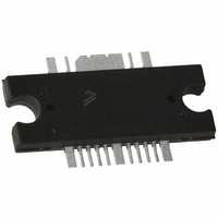
Manufacturer Part Number
MWIC930NR1
Description
IC PWR AMP RF 30W TO272-16
Manufacturer
Freescale Semiconductor
Type
Power Amplifierr
Datasheet
1.MWIC930NR1.pdf
(20 pages)
Specifications of MWIC930NR1
Current - Supply
90mA
Frequency
900MHz
Gain
30dB
Package / Case
TO-272-16
Rf Type
Cellular, GSM, EDGE, N-CDMA
Voltage - Supply
26V
Number Of Channels
1
Frequency (max)
960MHz
Output Power
30@960MHzdBm
Power Supply Requirement
Single
Single Supply Voltage (min)
26V
Single Supply Voltage (typ)
27V
Single Supply Voltage (max)
28V
Dual Supply Voltage (min)
Not RequiredV
Dual Supply Voltage (typ)
Not RequiredV
Dual Supply Voltage (max)
Not RequiredV
Pin Count
16
Mounting
Surface Mount
Lead Free Status / RoHS Status
Contains lead / RoHS Compliant
Noise Figure
-
P1db
-
Test Frequency
-
Lead Free Status / Rohs Status
Compliant
Other names
MWIC930NR1TR
Available stocks
Company
Part Number
Manufacturer
Quantity
Price
Company:

Part Number:
MWIC930NR1
Manufacturer:
FREESCALE
Quantity:
340
Part Number:
MWIC930NR1
Manufacturer:
FREESCALE
Quantity:
20 000


2
MWIC930R1 MWIC930GR1
Table 1. Maximum Ratings
Table 2. Thermal Characteristics
Table 3. ESD Protection Characteristics
Table 4. Moisture Sensitivity Level
Table 5. Electrical Characteristics
Functional Tests (In Freescale Test Fixture, 50 ohm system) V
f = 880 MHz, Single - Carrier N - CDMA, 1.2288 MHz Channel Bandwidth Carrier. ACPR measured in 30 kHz Bandwidth @ ±750 MHz Offset.
PAR = 9.8 dB @ 0.01% Probability on CCDF
Typical Performances (In Freescale Test Fixture) V
Drain- Source Voltage
Gate- Source Voltage
Storage Temperature Range
Operating Junction Temperature
Thermal Resistance, Junction to Case
Human Body Model
Machine Model
Charge Device Model
Per JESD 22 - A113, IPC/JEDEC J - STD - 020
Power Gain
Power Added Efficiency
Input Return Loss
Adjacent Channel Power Ratio
Quiescent Current Accuracy over Temperature
Gain Flatness in 80 MHz Bandwidth @ P
Deviation from Linear Phase in 80 MHz Bandwidth @ P
Delay @ P
Part - to - Part Phase Variation @ P
1. Refer to AN1955/D, Thermal Measurement Methodology of RF Power Amplifiers. Go to http://www.freescale.com/rf.
2. Refer to AN1977/D, Quiescent Current Thermal Tracking Circuit in the RF Integrated Circuit Family. Go to http://www.freescale.com/rf.
GSM Application
(P
GSM EDGE Application
(P
CDMA Application
(P
(f = 880 MHz)
Stage 1 with 33.2 kΩ Gate Feed Resistors ( - 30 to 115°C)
Stage 2 with 47.5 kΩ Gate Feed Resistors ( - 30 to 115°C)
Select Documentation/Application Notes - AN1955.
Select Documentation/Application Notes - AN1977.
out
out
out
= 30 W CW)
= 15 W CW)
= 5 W CW)
out
= 5 W CW Including Output Matching
Test Methodology
Characteristic
Test Conditions
out
Characteristic
= 5 W CW
Rating
(T
out
C
Stage 1, 26 Vdc, I
Stage 2, 26 Vdc, I
Stage 1, 27 Vdc, I
Stage 2, 27 Vdc, I
Stage 1, 27 Vdc, I
Stage 2, 27 Vdc, I
= 25°C, unless otherwise noted)
= 5 W CW
(2)
DD
= 26 Vdc, I
out
= 5 W CW
DQ
DQ
DQ
DQ
DQ
DQ
DD
= 90 mA
= 240 mA
= 90 mA
= 240 mA
= 90 mA
= 240 mA
DQ1
= 27 Vdc, I
= 90 mA, I
DQ1
Rating
Symbol
ACPR
Delay
ΔI
ΔI
PAE
G
IRL
DQ2
ΔΦ
3
G
= 90 mA, I
1QT
2QT
Φ
ps
F
= 240 mA, 840 MHz<Frequency<920 MHz
DQ2
Symbol
Symbol
Package Peak Temperature
Min
V
R
28
18
—
—
—
—
—
—
—
V
T
DSS
T
= 240 mA, P
θJC
GS
stg
J
260
±2.5
±2.5
Typ
±15
- 12
- 52
0.3
0.6
31
21
M3 (Minimum)
C2 (Minimum)
3
1 (Minimum)
out
- 65 to +175
Value
- 0.5, +65
- 0.5, +15
Value
Class
= 5 W Avg. N - CDMA,
200
Freescale Semiconductor
5.9
1.4
6.5
1.7
6.5
1.8
(1,2)
Max
- 48
—
—
—
—
—
—
—
- 9
RF Device Data
°C/W
(continued)
Unit
Unit
Vdc
Vdc
°C
°C
Unit
Unit
dBc
°C
dB
dB
dB
ns
%
%
°
°
Related parts for MWIC930NR1
Image
Part Number
Description
Manufacturer
Datasheet
Request
R

Part Number:
Description:
RF LDMOS Wideband Integrated Power Amplifiers
Manufacturer:
Motorola / Freescale Semiconductor

Part Number:
Description:
Manufacturer:
Freescale Semiconductor, Inc
Datasheet:
Part Number:
Description:
Manufacturer:
Freescale Semiconductor, Inc
Datasheet:
Part Number:
Description:
Manufacturer:
Freescale Semiconductor, Inc
Datasheet:
Part Number:
Description:
Manufacturer:
Freescale Semiconductor, Inc
Datasheet:
Part Number:
Description:
Manufacturer:
Freescale Semiconductor, Inc
Datasheet:
Part Number:
Description:
Manufacturer:
Freescale Semiconductor, Inc
Datasheet:
Part Number:
Description:
Manufacturer:
Freescale Semiconductor, Inc
Datasheet:
Part Number:
Description:
Manufacturer:
Freescale Semiconductor, Inc
Datasheet:
Part Number:
Description:
Manufacturer:
Freescale Semiconductor, Inc
Datasheet:
Part Number:
Description:
Manufacturer:
Freescale Semiconductor, Inc
Datasheet:
Part Number:
Description:
Manufacturer:
Freescale Semiconductor, Inc
Datasheet:
Part Number:
Description:
Manufacturer:
Freescale Semiconductor, Inc
Datasheet:
Part Number:
Description:
Manufacturer:
Freescale Semiconductor, Inc
Datasheet:
Part Number:
Description:
Manufacturer:
Freescale Semiconductor, Inc
Datasheet: