AMMP-6232-TR1G Avago Technologies US Inc., AMMP-6232-TR1G Datasheet
AMMP-6232-TR1G
Specifications of AMMP-6232-TR1G
Available stocks


Related parts for AMMP-6232-TR1G


AMMP-6232-TR1G Summary of contents
Page 1
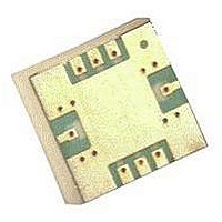
... GHz GaAs High Linearity LNA in SMT Package Data Sheet Description Avago’s AMMP-6232 is an easy-to-use broadband, high gain, high linearity Low Noise Amplifi surface mount package. The wide band and unconditionally stable performance makes this MMIC ideal as a primary or sub-sequential low noise block or a transmitter driver. ...
Page 2
... Ambient operational temperature TA=25°C unless noted 3. Channel-to-backside Thermal Resistance (Tchannel = 34°C) as measured using infrared microscopy. Thermal Resistance at backside temp. (Tb) = 25°C calculated from measured data. [4] AMMP-6232 RF Specifications TA= 25°C, Vdd = 4.0 V, Idd =135 mA, Zo=50 : Parameters and Test Conditions [5] Small-Signal Gain ...
Page 3
... AMMP-6232 Typical Performance (T = 25°C, Vdd=4V, Idd=138mA Frequency (GHz) Figure 1. Small-signal Gain Frequency (GHz) Figure 3. Input Return Loss 0 -5 -10 -15 -20 - Frequency (GHz) Figure 5. Output Return Loss Note: 1. S-parameters are measured on R&D Eval Board as shown in Figure 20. Effects of connectors and board traces are included in results. ...
Page 4
... AMMP-6232 Typical Performance (cont 25°C, Vdd=4V, Idd=138mA Frequency (GHz) Figure 7. Isolation Frequency (GHz) Figure 9. Gain over Vdd Frequency (GHz) Figure 11. Input Return Loss Over Vdd unless noted out 200 170 140 110 Figure 8. Total Current Figure 10. Noise Figure over Vdd - Figure 12. Output Return Loss Over Vdd 3 3 ...
Page 5
... AMMP-6232 Typical Performance (cont 25°C, Vdd=4V, Idd=138mA Frequency (GHz) Figure 13. Output P-1dB over Vdd Frequency (GHz) Figure 15. Gain over Temp Frequency (GHz) Figure 17. Input Return Loss Over Temp unless noted out Figure 14. Output IP3 Over Vdd 25C 85C 1 -40C Figure 16. Noise Figure over Temp ...
Page 6
... After adjusting the gate bias to obtain 138mA at Vdd = 4V, the AMMP-6232 can be safely biased (while fixing the gate bias) as desired. At 4V, the performance is an optimal compromise between power consumption, gain and power/linearity both applicable to be used as a low noise block or driver. At 3V, the amplifi ...
Page 7
... Recommended SMT Attachment for 5x5 Package Figure 22a. Suggested PCB Land Pattern and Stencil Layout Figure 22b. Stencil Outline Drawing (mm) The AMMP Packaged Devices are compatible with high volume surface mount PCB assembly processes. The PCB material and mounting pattern, as defined in the data sheet, optimizes RF performance and is strongly recommended ...
Page 8
... Figure 23. Suggested Lead-Free Reflow Profile for SnAgCu Solder Paste AMMP-6232 Part Number Ordering Information Devices Per Part Number Container AMMP-6232-BLKG 10 AMMP-6232-TR1G 100 AMMP-6232-TR2G 500 8 A properly designed solder screen or stencil is required to ensure optimum amount of solder paste is deposited onto the PCB pads. The recommended stencil layout is shown in Figure 22 ...
Page 9
... R 0.50 TYP. 1.75 ± 0.10 5.50 ± 0.05 Ø1.50 (MIN.) 8.00 ± 0. PITCH: WIDTH: Notes Pitches cumulative tolerance is ± 0.2 Mm. 3. Dimensions are in millimeters (mm). AMMP AMMP XXXX XXXX www.avagotech.com 0.114 (2.90) 0.018 (0.46) 0.014 (0.365 0.012 (0.30 0.028 (0.70) ...