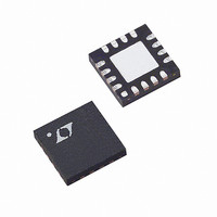
LT5515EUF Linear Technology, LT5515EUF Datasheet - Page 8

LT5515EUF
Manufacturer Part Number
LT5515EUF
Description
IC DEMODULATOR QUADRATURE 16-QFN
Manufacturer
Linear Technology
Datasheet
1.LT5515EUF.pdf
(12 pages)
Specifications of LT5515EUF
Function
Demodulator
Lo Frequency
1.5GHz ~ 2.5GHz
Rf Frequency
1.5GHz ~ 2.5GHz
P1db
9dBm
Gain
-0.7dB
Noise Figure
16.8dB
Current - Supply
160mA
Voltage - Supply
4 V ~ 5.25 V
Package / Case
16-QFN
Lead Free Status / RoHS Status
Contains lead / RoHS non-compliant
Available stocks
Company
Part Number
Manufacturer
Quantity
Price
Company:
Part Number:
LT5515EUF
Manufacturer:
LT
Quantity:
10 000
Company:
Part Number:
LT5515EUF#PBF
Manufacturer:
Linear Technology
Quantity:
135
Company:
Part Number:
LT5515EUF#PBF
Manufacturer:
LT
Quantity:
3 000
Part Number:
LT5515EUF#PBF
Manufacturer:
LINEAR/凌特
Quantity:
20 000
Part Number:
LT5515EUF#TRPBF
Manufacturer:
LINEAR/凌特
Quantity:
20 000
APPLICATIO S I FOR ATIO
LT5515
The LT5515 is a direct I/Q demodulator targeting high
linearity receiver applications, including wireless infra-
structure. It consists of an RF amplifier, I/Q mixers, a
quadrature LO carrier generator and bias circuitry.
The RF signal is applied to the inputs of the RF amplifier
and is then demodulated into I/Q baseband signals using
quadrature LO signals. The quadrature LO signals are
internally generated by precision 90° phase shifters. The
demodulated I/Q signals are lowpass filtered internally
with a –3dB bandwidth of 260MHz. The differential out-
puts of the I-channel and Q-channel are well matched in
amplitude; their phases are 90° apart.
RF Input Port
Differential drive is highly recommended for the RF inputs
to minimize the LO feedthrough to the RF port and to
maximize gain. (See Figure 2.) A 1:4 transformer is used
on the demonstration board for wider bandwidth match-
ing. To assure good NF and maximize the demodulator
gain, a low loss transformer is employed. Shunt inductor
L1, with high resonance frequency, is required for proper
impedance matching. Single-ended to differential conver-
sion can also be implemented using narrow band, discrete
L-C circuits to produce the required balanced waveforms
at the RF
the RF inputs is listed in Table 1.
Table 1. RF Input Differential Impedance
FREQUENCY
(GHz)
1.5
1.6
1.7
1.8
1.9
2.0
2.1
2.2
2.3
2.4
2.5
8
+
and RF
DIFFERENTIAL INPUT
IMPEDANCE (Ω)
115.7-j132.7
111.7-j128.1
108.1-j123.7
104.8-j120.2
101.7-j116.9
98.8-j113.8
96.0-j111.1
93.3-j108.7
90.7-j106.2
88.3-j104.2
85.9-j102.2
–
U
inputs.The differential impedance of
U
W
0.698
0.689
0.681
0.674
0.667
0.661
0.655
0.650
0.645
0.641
0.637
MAG
DIFFERENTIAL S11
ANGLE(°)
U
–24.9
–25.9
–26.8
–27.7
–28.5
–29.4
–30.2
–31.1
–32.0
–32.8
–33.7
The RF
1.54V. These two pins should be DC blocked when con-
nected to ground or other matching components. The RF
input equivalent circuit is shown in Figure 5.
A 4.3Ω resistor (R1) is connected to Pin 6 (V
optimum DC current for I/Q mixer linearity. The trade-off
of the NF and IIP3 as a function of R1 is shown in the
“Typical Performance Characteristics”. When a smaller
R1 is used for better linearity, the total supply current will
increase. A 5V ±5% power supply is recommended to
assure high linearity performance.
LO Input Port
The LO inputs (Pins 10,11) should be driven differentially
to minimize LO feedthrough to the RF port. This can be
accomplished by means of a single-ended to differential
conversion as shown in Figure 2. L4, the 12nH shunt
inductor, serves to tune out the capacitive component of
the LO differential input. The resonance frequency of the
inductor should be greater than the operating frequency.
A 1:2 transformer is used on the demo board to match the
LO port to a 50Ω source. Figure 6 shows the LO input
equivalent circuit and the associated matching network.
Single-ended to differential conversion at the LO inputs
can also be implemented using a discrete L-C circuit to
produce a balanced waveform without a transformer.
An alternative solution is a simple single-ended termina-
tion. However, the LO feedthrough to RF may be degraded.
Either LO
with a matching circuit, while the other input is connected
to ground through a 100pF bypass capacitor.
+
and RF
+
or LO
–
–
inputs (Pins 2, 3) are internally biased at
input can be terminated to a 50Ω source
CM
) to set the
5515fa


