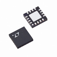
LT5515EUF Linear Technology, LT5515EUF Datasheet - Page 9

LT5515EUF
Manufacturer Part Number
LT5515EUF
Description
IC DEMODULATOR QUADRATURE 16-QFN
Manufacturer
Linear Technology
Datasheet
1.LT5515EUF.pdf
(12 pages)
Specifications of LT5515EUF
Function
Demodulator
Lo Frequency
1.5GHz ~ 2.5GHz
Rf Frequency
1.5GHz ~ 2.5GHz
P1db
9dBm
Gain
-0.7dB
Noise Figure
16.8dB
Current - Supply
160mA
Voltage - Supply
4 V ~ 5.25 V
Package / Case
16-QFN
Lead Free Status / RoHS Status
Contains lead / RoHS non-compliant
Available stocks
Company
Part Number
Manufacturer
Quantity
Price
Company:
Part Number:
LT5515EUF
Manufacturer:
LT
Quantity:
10 000
Company:
Part Number:
LT5515EUF#PBF
Manufacturer:
Linear Technology
Quantity:
135
Company:
Part Number:
LT5515EUF#PBF
Manufacturer:
LT
Quantity:
3 000
Part Number:
LT5515EUF#PBF
Manufacturer:
LINEAR/凌特
Quantity:
20 000
Part Number:
LT5515EUF#TRPBF
Manufacturer:
LINEAR/凌特
Quantity:
20 000
APPLICATIO S I FOR ATIO
Table 2 shows the differential input impedance of the LO
input port.
Table 2. LO Input Differential Impedance
FREQUENCY
(GHz)
1.5
1.6
1.7
1.8
1.9
2.0
2.1
2.2
2.3
2.4
2.5
I-Channel and Q-Channel Outputs
Each of the I-channel and Q-channel outputs is internally
connected to V
bias voltage is V
or AC coupled to the external loads. The differential output
impedance of the demodulator is 120Ω in parallel with a
5pF internal capacitor, forming a lowpass filter with a
–3dB corner frequency at 260MHz. R
DIFFERENTIAL INPUT
IMPEDANCE (Ω)
CC
CC
69.3-j59.4
64.3-j56.4
60.0-j52.7
56.4-j48.9
53.7-j44.9
51.4-j41.2
49.8-j37.5
48.6-j34.2
47.8-j31.0
47.3-j28.2
46.9-j25.6
though a 60Ω resistor. The output DC
– 0.85V. The outputs can be DC coupled
U
U
Figure 5. RF Input Equivalent Circuit with External Matching at 1.9GHz
RF
NOTE: NO CONNECTION REQUIRED
ACCORDING TO BALUN TRANSFORMER
MANUFACTURER
J1
W
0.469
0.457
0.440
0.421
0.399
0.377
0.352
0.328
0.303
0.279
0.257
MAG
DIFFERENTIAL S11
LDB311G9020C-452
LOAD
2
3
T1
(the single-
ANGLE (˚)
U
6
1
4
–45.8
–49.8
–53.9
–58.0
–62.2
–66.1
–69.9
–73.3
–76.5
–79.5
–82.3
C1
1nF
L1
10nH
ended load resistance) should be larger than 600Ω to
assure full gain. The gain is reduced by 20 • log(1 + 120Ω/
R
R
each output pin is connected to a 50Ω load (100Ω differ-
ential load). The output should be taken differentially (or
by using differential-to-single-ended conversion) for best
RF performance, including NF and IM2.
The phase relationship between the I-channel output sig-
nal and Q-channel output signal is fixed. When the LO
input frequency is larger (or smaller) than the RF input
frequency, the Q-channel outputs (Q
lag) I-channel outputs (I
When AC output coupling is used, the resulting highpass
filter’s –3dB roll-off frequency is defined by the R-C
constant of the blocking capacitor and R
R
Care should be taken when the demodulator’s outputs are
DC coupled to the external load, to make sure that the I/Q
mixers are biased properly. If the current drain from each
output exceeds 6mA, there can be significant degradation
of the linearity performance. Each output can sink no more
than 14mA when the outputs are connected to an external
load with a DC voltage higher than V
output equivalent circuit is shown in Figure 7.
2
3
LOAD
LOAD
LOAD
LT5515
RF
RF
+
–
) in dB when the differential output is terminated by
. For instance, the gain is reduced by 6.85dB when
V
> 600Ω.
CC
1.54V
1k
5515 F05
OUT
+
, I
OUT
–
) by 90°.
OUT
CC
+
– 0.85V. The I/Q
, Q
LOAD
LT5515
OUT
, assuming
–
) lead (or
5515fa
9


