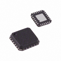
ADL5382ACPZ-R7 Analog Devices Inc, ADL5382ACPZ-R7 Datasheet - Page 14

ADL5382ACPZ-R7
Manufacturer Part Number
ADL5382ACPZ-R7
Description
IC DEMOD QUAD 700M2.7GHZ 24LFCSP
Manufacturer
Analog Devices Inc
Datasheet
1.ADL5382ACPZ-R7.pdf
(28 pages)
Specifications of ADL5382ACPZ-R7
Design Resources
Interfacing ADL5382 to AD9262 as an RF-to-Bits Solution (CN0062)
Function
Demodulator
Lo Frequency
700MHz ~ 2.7GHz
Rf Frequency
700MHz ~ 2.7GHz
P1db
14.5dBm
Gain
3.3dB
Noise Figure
17.6dB
Current - Supply
220mA
Voltage - Supply
4.75 V ~ 5.25 V
Package / Case
24-VFQFN, 24-CSP Exposed Pad
Frequency Range
700MHz To 2.7GHz
Rf Type
Quadrature
Supply Voltage Range
4.75V To 5.25V
Rf Ic Case Style
LFCSP
No. Of Pins
24
Operating Temperature Range
-40°C To +85°C
Lead Free Status / RoHS Status
Lead free / RoHS Compliant
Other names
ADL5382ACPZ-R7TR
Available stocks
Company
Part Number
Manufacturer
Quantity
Price
Company:
Part Number:
ADL5382ACPZ-R7
Manufacturer:
Analog Devices Inc
Quantity:
1 881
Part Number:
ADL5382ACPZ-R7
Manufacturer:
ADI/亚德诺
Quantity:
20 000
ADL5382
APPLICATIONS INFORMATION
BASIC CONNECTIONS
Figure 41 shows the basic connections schematic for the ADL5382.
POWER SUPPLY
The nominal voltage supply for the ADL5382 is 5 V and is
applied to the VPA, VPB, VPL, and VPX pins. Ground should
be connected to the COM, CML, and CMRF pins. The exposed
paddle on the underside of the package should also be soldered
to a low thermal and electrical impedance ground plane. If the
ground plane spans multiple layers on the circuit board, these
layers should be stitched together with nine vias under the
exposed paddle. The Application Note AN-772 discusses the
thermal and electrical grounding of the LFCSP in detail. Each
of the supply pins should be decoupled using two capacitors;
recommended capacitor values are 100 pF and 0.1 μF.
0.1µF
V
POS
0.1µF
V
POS
100pF
100pF
1
2
3
4
5
6
VPA
COM
BIAS
VPL
VPL
VPL
Figure 41. Basic Connections Schematic
LO
1000pF
24
7
RFC
1000pF
33nH
23
8
Rev. 0 | Page 14 of 28
ADL5382
ETC1-1-13
22
9
ETC1-1-13
1000pF
21
10
1000pF
33nH
20
11
LOCAL OSCILLATOR (LO) INPUT
For optimum performance, the LO port should be driven
differentially through a balun. The recommended balun is
the M/A-COM ETC1-1-13. The LO inputs to the device should
be ac-coupled with 1000 pF capacitors. The LO port is designed
for a broadband 50 Ω match from 700 MHz to 2.7 GHz. The
LO return loss can be seen in Figure 20. Figure 40 shows the LO
input configuration.
The recommended LO drive level is between −6 dBm and +6 dBm.
The applied LO frequency range is between 700 MHz and 2.7 GHz.
19
12
QLO
VPB
VPB
QHI
ILO
IHI
18
17
16
15
14
13
LO INPUT
100pF
ETC1-1-13
Figure 40. Differential LO Drive
ILO
IHI
QLO
0.1µF
QHI
V
POS
1000pF
1000pF
8
9
LOIP
LOIN


