ADL5500ACBZ-P7 Analog Devices Inc, ADL5500ACBZ-P7 Datasheet - Page 2
ADL5500ACBZ-P7
Manufacturer Part Number
ADL5500ACBZ-P7
Description
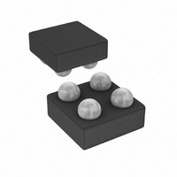
IC DETECTOR RF/IF TRUPWR 4WLCSP
Manufacturer
Analog Devices Inc
Datasheet
1.ADL5500ACBZ-P7.pdf
(24 pages)
Specifications of ADL5500ACBZ-P7
Frequency
100MHz ~ 6GHz
Rf Type
Cellular, CDMA2000, W-CDMA
Input Range
-18.5dBm ~ 6dBm
Accuracy
± 0.1dB
Voltage - Supply
2.7 V ~ 5.5 V
Current - Supply
1mA
Package / Case
4-WFBGA, WLCSP
Lead Free Status / RoHS Status
Lead free / RoHS Compliant
Other names
ADL5500ACBZ-P7
ADL5500ACBZ-P7TR
ADL5500ACBZ-P7TR
Available stocks
Company
Part Number
Manufacturer
Quantity
Price

Part Number:
ADL5500ACBZ-P7
Manufacturer:
ADI/亚德诺
Quantity:
20 000


ADL5500
TABLE OF CONTENTS
Features .............................................................................................. 1
Applications....................................................................................... 1
General Description ......................................................................... 1
Functional Block Diagram .............................................................. 1
Revision History ............................................................................... 2
Specifications..................................................................................... 3
Absolute Maximum Ratings............................................................ 7
Pin Configuration and Function Descriptions............................. 8
Typical Performance Characteristics ............................................. 9
Circuit Description......................................................................... 14
Applications..................................................................................... 15
REVISION HISTORY
2/06—Rev 0 to Rev. A
Changes to Features.......................................................................... 1
Changes to Table 2............................................................................ 7
Changes to Figure 5.......................................................................... 9
Changes to Figure 28 and Figure 31............................................. 13
Changes to Figure 35 Caption....................................................... 15
Changes to Power Consumption and Power-On/-Off
Response Section ............................................................................ 16
Changes to Figure 48...................................................................... 20
Changes to Ordering Guide .......................................................... 22
7/05—Revision 0: Initial Version
ESD Caution.................................................................................. 7
Filtering........................................................................................ 14
Basic Connections ...................................................................... 15
Output Swing .............................................................................. 15
Linearity....................................................................................... 15
Rev. A | Page 2 of 24
Outline Dimensions ....................................................................... 22
Input Coupling Using a Series Resistor................................... 16
Multiple RF Inputs ..................................................................... 16
Selecting the Output Low-Pass Filter Network ...................... 16
Power Consumption and Power-On/-Off Response............. 16
Output Drive Capability and Buffering................................... 17
VRMS Output Offset ................................................................. 17
Device Calibration and Error Calculation.............................. 18
Calibration for Improved Accuracy......................................... 18
Drift over a Reduced Temperature Range .............................. 19
Operation Above 4.0 GHz......................................................... 19
Device Handling......................................................................... 19
Evaluation Board ........................................................................ 20
Ordering Guide .......................................................................... 22
Related parts for ADL5500ACBZ-P7
Image
Part Number
Description
Manufacturer
Datasheet
Request
R

Part Number:
Description:
±1.7g Dual-Axis IMEMS Accelerometer Evaluation Board
Manufacturer:
Analog Devices Inc
Datasheet:

Part Number:
Description:
Inertial Sensor Evaluation System
Manufacturer:
Analog Devices Inc
Datasheet:
Part Number:
Description:
Manufacturer:
Analog Devices Inc
Datasheet:
Part Number:
Description:
Manufacturer:
Analog Devices Inc
Datasheet:
Part Number:
Description:
Manufacturer:
Analog Devices Inc
Datasheet:
Part Number:
Description:
Manufacturer:
Analog Devices Inc
Datasheet:
Part Number:
Description:
Manufacturer:
Analog Devices Inc
Datasheet:
Part Number:
Description:
Manufacturer:
Analog Devices Inc
Datasheet:
Part Number:
Description:
Manufacturer:
Analog Devices Inc
Datasheet:
Part Number:
Description:
Manufacturer:
Analog Devices Inc
Datasheet:
Part Number:
Description:
Manufacturer:
Analog Devices Inc
Datasheet:
Part Number:
Description:
Manufacturer:
Analog Devices Inc
Datasheet:
Part Number:
Description:
Manufacturer:
Analog Devices Inc
Datasheet: