AD8302ARU-REEL Analog Devices Inc, AD8302ARU-REEL Datasheet - Page 4
AD8302ARU-REEL
Manufacturer Part Number
AD8302ARU-REEL
Description
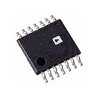
IC DETECTOR RF/IF 14-TSSOP T/R
Manufacturer
Analog Devices Inc
Datasheet
1.AD8302ARUZ.pdf
(24 pages)
Specifications of AD8302ARU-REEL
Rohs Status
RoHS non-compliant
Frequency
2.7GHz
Rf Type
General Purpose
Input Range
-60dBm ~ 0dBm
Accuracy
0.5dB
Voltage - Supply
2.7 V ~ 5.5 V
Current - Supply
23mA
Package / Case
14-TSSOP (0.173", 4.40mm Width)
Pin Count
14
Screening Level
Industrial
Package Type
TSSOP
Lead Free Status / Rohs Status
Not Compliant
Available stocks
Company
Part Number
Manufacturer
Quantity
Price

Part Number:
AD8302ARU-REEL7
Manufacturer:
ADI/亚德诺
Quantity:
20 000


AD8302
ABSOLUTE MAXIMUM RATINGS
Supply Voltage V
PSET, MSET Voltage . . . . . . . . . . . . . . . . . . . . . . V
INPA, INPB Maximum Input . . . . . . . . . . . . . . . . . . –3 dBV
θ
Maximum Junction Temperature . . . . . . . . . . . . . . . . 125°C
Operating Temperature Range . . . . . . . . . . . –40°C to +85°C
Storage Temperature Range . . . . . . . . . . . . –65°C to +150°C
Lead Temperature Range (Soldering 60 sec) . . . . . . . . 300°C
NOTES
Pin No.
1, 7
2
3
4
5
6
8
9
10
11
12
13
14
CAUTION
ESD (electrostatic discharge) sensitive device. Electrostatic charges as high as 4000 V readily
accumulate on the human body and test equipment and can discharge without detection. Although
the AD8302 features proprietary ESD protection circuitry, permanent damage may occur on
devices subjected to high energy electrostatic discharges. Therefore, proper ESD precautions are
recommended to avoid performance degradation or loss of functionality.
1
2
nent damage to the device. This is a stress rating only; functional operation of the
device at these or any other conditions above those indicated in the operational
section of this specification is not implied. Exposure to absolute maximum rating
conditions for extended periods may affect device reliability.
Stresses above those listed under Absolute Maximum Ratings may cause perma-
JEDEC 1S Standard (2-layer) board data.
JA
Equivalent Power Re. 50 Ω . . . . . . . . . . . . . . . . . . 10 dBm
2
. . . . . . . . . . . . . . . . . . . . . . . . . . . . . . . . . . . . . 150°C/W
Model
AD8302ARU
AD8302ARU-REEL
AD8302ARU-REEL7
AD8302-EVAL
Mnemonic
COMM
INPA
OFSA
VPOS
OFSB
INPB
PFLT
VPHS
PSET
VREF
MSET
VMAG
MFLT
S
. . . . . . . . . . . . . . . . . . . . . . . . . . . . . 5.5 V
1
Function
Device Common. Connect to low impedance ground.
High Input Impedance to Channel A. Must be ac-coupled.
A capacitor to ground at this pin sets the offset compensation filter corner
and provides input decoupling.
Voltage Supply (V
A capacitor to ground at this pin sets the offset compensation filter corner
and provides input decoupling.
Input to Channel B. Same structure as INPA.
Low Pass Filter Terminal for the Phase Output
Single-Ended Output Proportional to the Phase Difference between INPA
and INPB.
Feedback Pin for Scaling of VPHS Output Voltage in Measurement Mode.
Apply a setpoint voltage for controller mode.
Internally Generated Reference Voltage (1.8 V Nominal)
Feedback Pin for Scaling of VMAG Output Voltage Measurement Mode.
Accepts a set point voltage in controller mode.
Single-Ended Output. Output voltage proportional to the decibel ratio
of signals applied to INPA and INPB.
Low Pass Filter Terminal for the Magnitude Output
–40°C to +85°C
Temperature Range
PIN FUNCTION DESCRIPTIONS
S
ORDERING GUIDE
+ 0.3 V
S
), 2.7 V to 5.5 V
–4–
13" Tape and Reel
7" Tape and Reel
Evaluation Board
Package Description
Tube, 14-Lead TSSOP
COMM
COMM
PIN CONFIGURATION
OFSA
VPOS
OFSB
INPA
INPB
1
2
3
4
5
6
7
(Not to Scale)
TOP VIEW
AD8302
Package
Option
RU-14
WARNING!
14
13
12
11
10
9
8
MFLT
VMAG
MSET
VREF
PSET
VPHS
PFLT
ESD SENSITIVE DEVICE
Equivalent
Circuit
Circuit A
Circuit A
Circuit A
Circuit A
Circuit E
Circuit B
Circuit D
Circuit C
Circuit D
Circuit B
Circuit E
REV. A
Related parts for AD8302ARU-REEL
Image
Part Number
Description
Manufacturer
Datasheet
Request
R

Part Number:
Description:
IC DETECTOR RF/IF 14-TSSOP
Manufacturer:
Analog Devices Inc
Datasheet:
Part Number:
Description:
IC,Phase/Frequency Detector,BIPOLAR,TSSOP,14PIN,PLASTIC
Manufacturer:
Analog Devices Inc
Datasheet:

Part Number:
Description:
LF.2.7 GHz RF/IF Gain and Phase Detector
Manufacturer:
Analog Devices
Datasheet:

Part Number:
Description:
±1.7g Dual-Axis IMEMS Accelerometer Evaluation Board
Manufacturer:
Analog Devices Inc
Datasheet:

Part Number:
Description:
Inertial Sensor Evaluation System
Manufacturer:
Analog Devices Inc
Datasheet:
Part Number:
Description:
Manufacturer:
Analog Devices Inc
Datasheet:
Part Number:
Description:
Manufacturer:
Analog Devices Inc
Datasheet:
Part Number:
Description:
Manufacturer:
Analog Devices Inc
Datasheet:
Part Number:
Description:
Manufacturer:
Analog Devices Inc
Datasheet:
Part Number:
Description:
Manufacturer:
Analog Devices Inc
Datasheet:
Part Number:
Description:
Manufacturer:
Analog Devices Inc
Datasheet:
Part Number:
Description:
Manufacturer:
Analog Devices Inc
Datasheet: