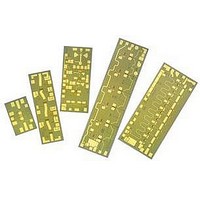
AMMC-6120-W50 Avago Technologies US Inc., AMMC-6120-W50 Datasheet - Page 6

AMMC-6120-W50
Manufacturer Part Number
AMMC-6120-W50
Description
IC MMIC FREQ MULTIPLIER 6-20GHZ
Manufacturer
Avago Technologies US Inc.
Datasheet
1.AMMC-6120-W50.pdf
(8 pages)
Specifications of AMMC-6120-W50
Function
Frequency Multiplier
Supply Current
85mA
Supply Voltage Range
5V
Frequency Max
10GHz
Frequency Min
4GHz
Supply Voltage Max
7V
Gain
1dB
Manufacturer's Type
MMIC Amplifier
Number Of Channels
1
Frequency (max)
20GHz
Operating Supply Voltage (typ)
5V
Package Type
Chip
Mounting
Surface Mount
Lead Free Status / RoHS Status
Lead free / RoHS Compliant
Lead Free Status / RoHS Status
Lead free / RoHS Compliant, Lead free / RoHS Compliant
Available stocks
Company
Part Number
Manufacturer
Quantity
Price
Part Number:
AMMC-6120-W50
Manufacturer:
AVAGO/安华高
Quantity:
20 000
Figure. 19 2H Output Power Vs Input Power @ Fout=26GHz
Figure.21 SSB Phase Noise of frequency doubler
(Pin=+2dBm, fout=15.6GHz)
Biasing and Operation
The frequency doubler MMIC consists of a differen-
tial amplifier circuit that acts as an active balun. The
outputs of this balun feed the gates of balanced FETs
and the drains are connected to form the single-ended
output. This results in the fundamental frequency and
odd harmonics canceling and the even harmonic drain
currents (in phase) adding in superposition. Node ‘S’ acts
as a virtual ground. An input matching network (M/N)
is designed to provide good match at fundamental fre-
quencies and produces high impedance mismatch at
higher harmonics.
AMMC-6120 is biased with a single positive drain supply
and single negative gate supply using separate bypass
capacitors. It is normally biased with the drain supply
connected to both the VdAB and the Vdd bond pads
and the gate supply connected to the VgD bond pad. It
is important to bypass both VdAB and Vdd with 100 pF
capacitors placed as close to the die as possible. Typical
bias connections are shown in Figure 22. For most of the
application it is recommended to use a Vg = –1.2 V and
Vd = 4.5 V.
6
20
18
16
14
12
10
-100
-110
-120
-130
-140
-150
-160
-170
8
6
4
2
0
-50
-60
-70
-80
-90
1.E+02
-11 -9
Fout=26GHz
Vd=4.5V, Vg=-1.2V
-7
1.E+03
-5
Input Power [1H] (dBm)
-3
Offset Frequency [Hz]
1.E+04
-1
1
1.E+05
Vg=-1.2V, Vd=4.5V
Vg=-1.2V, Vd=5.0V
Vg=-1.4V, Vd=4.5V
Vg=-1.4V, Vd=5.0V
3
Fout=15.6GHz
5
1.E+06
7
9
1.E+07
11
Figure 22.
Figure. 20 Fundamental Supp. Vs Input Power @ Fout=26GHz
The AMMC-6120 performance changes very slightly with
Drain (Vd) and Gate bias (Vg) as shown in Figure 8 and 9.
Minor improve-ments in performance are possible for
output power or fundamental suppression by optimizing
the Vg from –1.0 V to –1.4 V and/or Vd from 4.0 to 5.0 V.
The RF input and output port are AC coupled thus no
DC voltage is present at either ports. However, the RF
output port has a internal output-matching circuit that
presents a DC short. Proper care should be taken while
biasing sequential circuit to AMMC-6120 as it might cause
DC short (use a DC block if sub sequential circuit is not
AC coupled). No ground wires are needed since ground
connections are made with plated through-holes to the
backside of the device.
Refer the Absolute Maximum Ratings table for allowed
DC and thermal conditions.
35
10
15
20
25
30
5
-11
M/N
@ fo
-9
A. DIFF. AMP
ACTIVE BALUN
-7
-5
Input Power [1H] (dBm)
Fout=26GHz
-3
-1
Vg=-1.2V, Vd=4.5V
Vg=-1.2V, Vd=5.0V
Vg=-1.4V, Vd=4.5V
Vg=-1.4V, Vd=5.0V
S
1
3
M/N
@ 2fo
5
7
9
11


