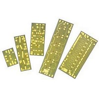
AMMC-6222-W50 Avago Technologies US Inc., AMMC-6222-W50 Datasheet - Page 11

AMMC-6222-W50
Manufacturer Part Number
AMMC-6222-W50
Description
IC MMIC LNA 7GHZ-21GHZ
Manufacturer
Avago Technologies US Inc.
Datasheet
1.AMMC-6222-W10.pdf
(12 pages)
Specifications of AMMC-6222-W50
Function
Amplifier
Frequency Range
7GHz To 21GHz
Noise Figure Typ
2.4dB
Supply Current
120mA
Supply Voltage Range
3V To 5V
Frequency Max
21GHz
Frequency Min
7GHz
Supply Voltage Max
5V
Gain
25dB
Number Of Channels
1
Power Supply Requirement
Single
Single Supply Voltage (min)
3V
Single Supply Voltage (typ)
4V
Single Supply Voltage (max)
5V
Package Type
Chip
Dual Supply Voltage (min)
Not RequiredV
Dual Supply Voltage (typ)
Not RequiredV
Dual Supply Voltage (max)
Not RequiredV
Mounting
Surface Mount
Lead Free Status / RoHS Status
Lead free / RoHS Compliant
Lead Free Status / RoHS Status
Lead free / RoHS Compliant, Lead free / RoHS Compliant
AMMC-6222 Application and Usage
Figure 19. Low Current, Low Output Power State
Figure 20. High Current, High Output Power State
Figure 21. Simplified High Linearity LNA Schematic
RF INPUT
RF INPUT
>= 100 pF Capacitor
>= 100 pF Capacitor
Gold Plated Shim (Optional)
Gold Plated Shim (Optional)
V
V
D1
D1
AMMC-6222
AMMC-6222
V
V
To V
Open
To V
D2
D2
DD
DD
DC supply
DC supply
RF OUTPUT
RF OUTPUT
Biasing and Operation
The AMMC-6222 is normally biased with a positive drain
supply connected to the VD1 and VD2 pads through
bypass capacitor as shown in Figures 19 and 20. The
recommended drain supply voltage for general usage is
4V and the corresponding drain current is approximately
120mA. It is important to have at least 100pF bypass
capacitor and the capacitor should be placed as close
to the component as possible. Aspects of the amplifier
performance may be improved over a narrower
bandwidth by application of additional conjugate,
linearity, or low noise (Topt) matching.
For receiver front end low noise applications where high
power and linearity are not often required, the AMMC-
6222 can be set in low current state when SELECT pad
is open as shown in Figure 19. In this configuration, the
bias current is approximately 85mA, 95mA and 105mA
for 3V, 4V and 5V respectively.
In applications where high output power and linearity
are often required such as LO or transmitter drivers, the
AMMC-6222 can be selected to operate at its highest
output power by grounding SELECT pad as shown in
Figure 20. At 5V, the amplifier can provide Psat of about
20dBm. The bias current in this configuration is 115mA,
120mA and 125mA for 3V, 4V and 5V respectively.
In both cases, bonding wires at the input and output in
the range of 0.15nH would likely improve the overall Noise
Figure and input, output match at most frequencies.
No ground wires are needed because all ground
connections are made with plated through-holes to the
backside of the substrate.
Refer the Absolute Maximum Ratings table for allowed
DC and thermal condition.


