MICRF505DEV1 Micrel Inc, MICRF505DEV1 Datasheet - Page 12
MICRF505DEV1
Manufacturer Part Number
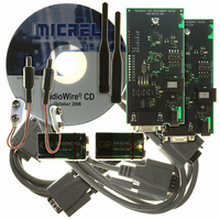
MICRF505DEV1
Description
KIT DEV RADIOWIRE 850-950MHZ
Manufacturer
Micrel Inc
Series
RadioWire®r
Type
Transceiver, ISMr
Specifications of MICRF505DEV1
Frequency
850MHz ~ 950MHz
For Use With/related Products
MICRF505
Lead Free Status / RoHS Status
Lead free / RoHS Compliant
Other names
576-1606
Available stocks
Company
Part Number
Manufacturer
Quantity
Price
Company:

Part Number:
MICRF505DEV1
Manufacturer:
Micrel Inc
Quantity:
135


Writing to n Registers having Non-Incremental
Addresses
Registers with non-incremental addresses can be
written to in one write-sequence as well. Example of
non-incremental addresses: “0,1,3”. However, this
requires more overhead, and the user should
consider the possibility to make a “continuous”
update, for example, by writing to “0,1,2,3” (writing
the present value of “2” into “2”). The simplest
firmware is achieved by always writing to all
registers. Refer to previous sections.
This write-sequence is divided into several sub-
parts:
Refer to the previous sections for how to write to 1 or
n (with incremental addresses) registers in the
MICRF505.
Reading from the control registers in MICRF505
The “read-sequence” is:
It is possible to read all, 1 or n registers. The
address to read from (or the first address to read
from) can be any valid address (0-22). Reading is
not destructive, i.e. values are not changed. The IO
line is output from the MICRF505 (input to user) for a
part of the read-sequence. Refer to procedure
description below.
A read-sequence is described for reading n
registers, where n is number 1-23.
Micrel
October 2006
•
•
1. Enter address and R/W bit
2. Change direction of IO line
3. Read out a number of octets and change IO
Disable the generation of load-signals by
clearing
ControlRegister0)
Repeat for each group of register having
incremental addresses:
direction back again.
o
o
o
o
Bring CS active
Enter first address for this group,
R/W bit and values
Bring CS inactive
Finally, enable and make a load-
signal by setting “load_en”
bit
“load_en”
(bit0
in
12
Reading n registers from MICRF505
Simple time
IO Input
IO Output
In the figure, 1 register is read. The address is A6,
A5, … A0. A6 = msb. The data read out is D7, D6,
…D0. The value of the R/W bit is always “1” for
reading.
SCLK and IO together form a serial interface. SCLK
is applied externally for reading as well as for writing.
Programming interface timing
Figure 4 and Table 6 shows the timing specification
for the 3-wire serial programming interface.
SCLK
CS
IO
•
•
•
•
•
•
CS
SCLK
IO
Tcsr
Bring CS active
Enter address to read from (or the first
address to read from) (7 bits) and
The R/W bit = 1 to enable reading
Make the IO line an input to the user (set pin
in tristate)
Read n octets. The first rising edge of SCLK
will set the IO as an output from the
MICRF505. MICRF will change the IO line at
positive edges. The user should read the IO
line at the negative edges.
Make the IO line an output from the user
again.
A6
Address Register
traise
Address of register i
A6
A5
tfall
A5
Figure 3.
Figure 4.
Tper
A0
A0
RW
Tlow
RW D7
RWData read from reg. i
Thigh
MICRF505BML/YML
D7
Tread
+1 408-944-0800
D6
D6
M9999-103106
Data Register
D0
Twrite
D2
D1
D0
LOAD
Tscl
Related parts for MICRF505DEV1
Image
Part Number
Description
Manufacturer
Datasheet
Request
R

Part Number:
Description:
Manufacturer:
Micrel Inc
Datasheet:
Part Number:
Description:
Manufacturer:
Micrel Inc
Datasheet:
Part Number:
Description:
Manufacturer:
Micrel Inc
Datasheet:
Part Number:
Description:
Manufacturer:
Micrel Inc
Datasheet:
Part Number:
Description:
Manufacturer:
Micrel Inc
Datasheet:
Part Number:
Description:
Manufacturer:
Micrel Inc
Datasheet:
Part Number:
Description:
Manufacturer:
Micrel Inc
Datasheet:
Part Number:
Description:
Manufacturer:
Micrel Inc
Datasheet:
Part Number:
Description:
Manufacturer:
Micrel Inc
Datasheet:
Part Number:
Description:
Manufacturer:
Micrel Inc
Datasheet:
Part Number:
Description:
Manufacturer:
Micrel Inc
Datasheet:
Part Number:
Description:
Manufacturer:
Micrel Inc
Datasheet:
Part Number:
Description:
Manufacturer:
Micrel Inc
Datasheet:
Part Number:
Description:
Manufacturer:
Micrel Inc
Datasheet: