EVB71102B-433-FSK-C Melexis Inc, EVB71102B-433-FSK-C Datasheet - Page 4
EVB71102B-433-FSK-C
Manufacturer Part Number
EVB71102B-433-FSK-C
Description
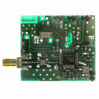
EVALUATION BOARD TH71102 RECEIVR
Manufacturer
Melexis Inc
Type
Receiver, ASK/FSKr
Specifications of EVB71102B-433-FSK-C
Rohs Status
RoHS non-compliant
Frequency
433MHz
For Use With/related Products
TH71102
Other names
EVB71102-433-FSK
EVB71102-433-FSK
EVB71102-433.92F
EVB71102-433.92F
EVB71102B-433FSKC
EVB71102-433-FSK
EVB71102-433.92F
EVB71102-433.92F
EVB71102B-433FSKC


1.3 Block Diagram
1.4 Mode Configurations
Note: ENRX are pulled down internally
1.5 LNA GAIN Control
Note: hysteresis between gain modes to ensure stability
1.6 Frequency Planning
Frequency planning is straightforward for single-conversion applications because there is only one IF that
can be chosen, and then the only possible choice is low-side or high-side injection of the LO signal (which is
now the one and only LO signal in the receiver).
The receiver’s double-conversion architecture requires careful frequency planning. Besides the desired RF
input signal, there are a number of spurious signals that may cause an undesired response at the output.
Among them are the image of the RF signal (that must be suppressed by the RF front-end filter), spurious
signals injected to the first IF (IF1) and their images which could be mixed down to the same second IF (IF2)
as the desired RF signal (they must be suppressed by the LC filter at IF1 and/or by low-crosstalk design).
39012 71102 01
Rev. 012
V
< 0.8 V
> 1.4 V
IN_LNA
31
ENRX
GAIN_LNA
32
1
0
1
LNA
30
2
3
4
VCO1
MIX1
DIV8
5
LO1
HIGH GAIN
RX standby
LOW GAIN
RX active
29
6
Mode
Mode
LF
DIV2
IF1
Fig. 1: TH71102 block diagram
7
CP
MIX2
8
PFD
LO2
9
Page 4 of 14
IF2
10
26
RO
RO
11
12
25
13
27
Evaluation Board Description
IFA
21
28
LNA set to high gain
LNA set to low gain
BIAS
14
Description
Description
RX disabled
RX enable
15
315/433MHz Receiver
22
MIX3
EVB71102
16
17
EVB Description
OA
OUT_OA
OUTN
OUTP
OAN
OAP
23
24
20
19
18
April/08
Related parts for EVB71102B-433-FSK-C
Image
Part Number
Description
Manufacturer
Datasheet
Request
R

Part Number:
Description:
EVALUATION BOARD TH71102 RECEIVR
Manufacturer:
Melexis Inc
Datasheet:

Part Number:
Description:
EVALUATION BOARD TH71102 RECEIVR
Manufacturer:
Melexis Inc
Datasheet:
Part Number:
Description:
Evaluation Board For Th71102
Manufacturer:
Melexis Company
Datasheet:
Part Number:
Description:
315/433MHz Receiver Evaluation Board Description
Manufacturer:
MELEXIS [Melexis Microelectronic Systems]
Datasheet:

Part Number:
Description:
IC LATCH CMOS MP TSOT23-3
Manufacturer:
Melexis Inc
Datasheet:

Part Number:
Description:
IC LATCH CMOS MP TSOT23-3
Manufacturer:
Melexis Inc
Datasheet:
Part Number:
Description:
IC HALL EFFECT SW TSOT-23
Manufacturer:
Melexis Inc
Datasheet:

Part Number:
Description:
IC HALL EFFECT SWITCH TSOT-23
Manufacturer:
Melexis Inc
Datasheet: