1321XEVK Freescale Semiconductor, 1321XEVK Datasheet - Page 20
1321XEVK
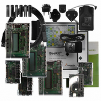
Manufacturer Part Number
1321XEVK
Description
KIT EVALUATION FOR 1321X
Manufacturer
Freescale Semiconductor
Type
Zigbeer
Specifications of 1321XEVK
Frequency
2.4GHz
Wireless Frequency
2.4 GHz
Modulation
DSSS OQPSK
Security
128 bit AES
Operating Voltage
2 VDC to 3.4 VDC
Operating Temperature Range
- 40 C to + 85 C
For Use With/related Products
MC1321x
Lead Free Status / RoHS Status
Contains lead / RoHS non-compliant


4.6.2
The MCU directs the 802.15.4 modem, checks its status, and reads/writes data to the device through the
4-wire SPI port. The transceiver operates as a SPI slave device only. A transaction between the host and
the 802.15.4 modem occurs as multiple 8-bit bursts on the SPI. The modem SPI signals are:
Although the SPI port is fully static, internal memory, timer and interrupt arbiters require an internal clock
(CLK
registers and memory.
4.6.2.1
The SPI port of the MCU transfers data in bursts of 8 bits with most significant bit (MSB) first. The master
(MCU) can send a byte to the slave (transceiver) on the MOSI line and the slave can send a byte to the
master on the MISO line. Although an 802.15.4 modem transaction is three or more SPI bursts long, the
timing of a single SPI burst is shown in
because the modem is limited by this number.
20
1. Chip Enable (CE) - A transaction on the SPI port is framed by the active low CE input signal. A
2. SPI Clock (SPICLK) - The host drives the SPICLK input to the 802.15.4 modem. Data is clocked
3. Master Out/Slave In (MOSI) - Incoming data from the host is presented on the MOSI input.
4. Master In/Slave Out (MISO) - The 802.15.4 modem presents data to the master on the MISO
core
SPICLK
CE
MISO
MOSI
transaction is a minimum of 3 SPI bursts and can extend to a greater number of bursts.
into the master or slave on the leading (rising) edge of the return-to-zero SPICLK and data out
changes state on the trailing (falling) edge of SPICLK.
output.
), derived from the crystal reference oscillator, to communicate from the SPI registers to internal
Serial Peripheral Interface (SPI)
SPI Burst Operation
For the MCU, the SPI clock format is the clock phase control bit CPHA = 0
and the clock polarity control bit CPOL = 0.
Valid
1
Valid
Figure 10. SPI Single Burst Timing Diagram
2
MC13211/212/213 Technical Data, Rev. 1.8
Figure
3
10. The maximum SPI clock rate is 8 Mhz from the MCU
NOTE
4
SPI Burst
5
6
7
Freescale Semiconductor
8
Related parts for 1321XEVK
Image
Part Number
Description
Manufacturer
Datasheet
Request
R

Part Number:
Description:
Manufacturer:
Freescale Semiconductor, Inc
Datasheet:
Part Number:
Description:
Manufacturer:
Freescale Semiconductor, Inc
Datasheet:
Part Number:
Description:
Manufacturer:
Freescale Semiconductor, Inc
Datasheet:
Part Number:
Description:
Manufacturer:
Freescale Semiconductor, Inc
Datasheet:
Part Number:
Description:
Manufacturer:
Freescale Semiconductor, Inc
Datasheet:
Part Number:
Description:
Manufacturer:
Freescale Semiconductor, Inc
Datasheet:
Part Number:
Description:
Manufacturer:
Freescale Semiconductor, Inc
Datasheet:
Part Number:
Description:
Manufacturer:
Freescale Semiconductor, Inc
Datasheet:
Part Number:
Description:
Manufacturer:
Freescale Semiconductor, Inc
Datasheet:
Part Number:
Description:
Manufacturer:
Freescale Semiconductor, Inc
Datasheet:
Part Number:
Description:
Manufacturer:
Freescale Semiconductor, Inc
Datasheet:
Part Number:
Description:
Manufacturer:
Freescale Semiconductor, Inc
Datasheet:
Part Number:
Description:
Manufacturer:
Freescale Semiconductor, Inc
Datasheet:
Part Number:
Description:
Manufacturer:
Freescale Semiconductor, Inc
Datasheet:
Part Number:
Description:
Manufacturer:
Freescale Semiconductor, Inc
Datasheet: