MDEV-900-HP3-PPS-RS232 Linx Technologies Inc, MDEV-900-HP3-PPS-RS232 Datasheet - Page 5
MDEV-900-HP3-PPS-RS232
Manufacturer Part Number
MDEV-900-HP3-PPS-RS232
Description
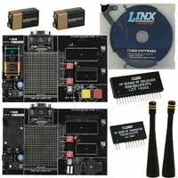
KIT MASTER 900MHZ HP-3 SIP RS232
Manufacturer
Linx Technologies Inc
Series
HP3r
Type
Receiverr
Datasheet
1.MDEV-900-HP3-PPS-RS232.pdf
(13 pages)
Specifications of MDEV-900-HP3-PPS-RS232
Frequency
902MHz ~ 928MHz
For Use With/related Products
HP3 Series RF Modules
Lead Free Status / RoHS Status
Contains lead / RoHS non-compliant
Other names
MDEV-900-HP3
MDEV-900-HP3
MDEV-900-HP3-PPS
MDEV-900-HP3-PPS
MDEV900HP3
MDEV900HP3PPSRS23
MDEV-900-HP3
MDEV-900-HP3-PPS
MDEV-900-HP3-PPS
MDEV900HP3
MDEV900HP3PPSRS23


THE DATA OUTPUT
AUDIO OUTPUT
Figure 12: Audio Buffer Amplifier
Page 8
HP Analog Out
The DATA line outputs recovered digital data. It is an open collector output with
an internal 4.7kΩ pull-up. When an RF transmission is not present, or when the
received signal strength is too low to ensure proper demodulation, the data
output is squelched continuous high. This feature supports direct operation with
UARTs, which require their input to be continuously high. An HP3 transmitter and
receiver can be directly connected between two UARTs without the need for
buffering or logical inversion. It should be noted that the squelch level is set just
over the receiver’s internal noise threshold. Any external RF activity above that
threshold will “break squelch” and produce hashing on the line. While the DATA
line will be reliably squelched in low-noise environments, the designer should
always plan for the potential of hashing.
The HP3 Series is optimized for the transmission of serial data; however, it can
also be used very effectively to send a variety of analog signals, including audio.
The ability of the HP3 to send combinations of audio and data opens new areas
of opportunity for creative design.
The analog output of the AUDIO line is valid from 50 Hz to 28 kHz, providing an
AC signal of about 1V peak-to-peak. This is a high impedance output and not
suitable for directly driving low-impedance loads, such as a speaker. In
applications where a low impedance load is to be driven, a buffer circuit should
always be used. For example, in the case of a speaker, a simple op-amp circuit
such as the one shown below can be used to act as an impedance converter.
The transmitter’s modulation voltage is critical, since it determines the carrier
deviation and distortion. The transmitter input level should be adjusted to
achieve the optimum results for your application in your circuit. Please refer to
the transmitter data guide for full details.
When used for audio, the analog output of the receiver should be filtered and
buffered to obtain maximum sound quality. For voice, a 3-4kHz low-pass filter is
often employed. For broader-range sources, such as music, a 12-17kHz cutoff
may be more appropriate. In applications that require high-quality audio, a
compandor may be used to further improve SNR. The HP3 is capable of
providing audio quality comparable to a radio or intercom. For applications where
true high fidelity audio is required, the HP3 will probably not be the best choice,
and a device optimized for audio should be utilized.
1uF
10k
2
3
+
VCC
–
6
4
LM386
5
0.05uF
10 ohm
250uF
TIMING CONSIDERATIONS
RECEIVING DATA
Parameter
There are four major timing considerations to be aware of when designing with
the HP3 Series receiver. These are shown in the table below.
T1 is the maximum amount of time that can elapse without a data transition. Data
must always be considered in both the analog and the digital domain. Because
the data stream is asynchronous and no particular format is imposed, it is
possible for the data to meet the receiver’s data rate requirement yet violate the
analog frequency requirements. For example, if a 255 (0FF hex) were sent
continuously, the receiver would view the data as a DC level. It would hold that
level until a transition was required to meet the minimum frequency specification.
If no transition occurred, data integrity could not be guaranteed. While no
particular structure or balancing requirement is imposed, the designer must
ensure that both analog and digital signals meet the transition specification.
T2 is the worst-case time needed for a powered-up module to switch between
channels after a valid channel selection. This time does not include external
overhead for loading a desired channel in the serial channel-selection mode.
T3 is the time to receiver readiness from the PDN line going high. Receiver
readiness is determined by valid data on the DATA line. This assumes an
incoming data stream and the presence of stable supply on V
T4 is the time to receiver readiness from the application of V
readiness is determined by valid data on the DATA line. This assumes an
incoming data stream and the PDN line is high or open.
Once an RF link has been established, the challenge becomes how to effectively
transfer data across it. While a properly designed RF link provides reliable data
transfer under most conditions, there are still distinct differences from a wired link
that must be addressed. Since the modules do not incorporate internal encoding
or decoding, the user has tremendous flexibility in how data is handled.
It is important to separate the types of transmissions that are technically possible
from those that are legally allowed in the country of operation. Application Notes
AN-00126, AN-00140 and Part 15, Section 249 of the FCC rules should be
reviewed for details on acceptable transmission content in the U.S.
If you want to transfer simple control or status signals (such as button presses)
and your product does not have a microprocessor or you wish to avoid protocol
development, consider using an encoder / decoder IC set. These chips are
available from several manufacturers, including Linx. They take care of all
encoding and decoding functions and provide a number of data lines to which
switches can be directly connected. Address bits are usually provided for
security and to allow the addressing of multiple receivers independently. These
ICs are an excellent way to bring basic remote control products to market quickly
and inexpensively. It is also a simple task to interface with inexpensive
microprocessors or one of many IR, remote control, DTMF, or modem ICs.
T1
T2
T3
T4
Channel change time (time to valid data)
Time between DATA output transitions
Receiver turn-on time via PDN
Receiver turn-on time via V
Description
CC
CC
.
CC
20.0mS
. Receiver
1.5mS
3.0mS
7.0mS
Max.
Page 9
Related parts for MDEV-900-HP3-PPS-RS232
Image
Part Number
Description
Manufacturer
Datasheet
Request
R

Part Number:
Description:
KIT MASTER 900MHZ HP-3 RS232 SMD
Manufacturer:
Linx Technologies Inc
Datasheet:

Part Number:
Description:
KIT MASTER 900MHZ HP-3 USB SMD
Manufacturer:
Linx Technologies Inc
Datasheet:

Part Number:
Description:
KIT MASTER 900MHZ HP-3 USB PIN
Manufacturer:
Linx Technologies Inc
Datasheet:

Part Number:
Description:
HOLDER BATTERY 20MM COIN CR2032
Manufacturer:
Linx Technologies Inc
Datasheet:

Part Number:
Description:
CONN RPSMA BL CRJA-CPV 8.5" COAX
Manufacturer:
Linx Technologies Inc

Part Number:
Description:
CABLE RG174 RPSMA M/F 8.5"
Manufacturer:
Linx Technologies Inc

Part Number:
Description:
CABLE RG174 SMA M/F 8.5"
Manufacturer:
Linx Technologies Inc

Part Number:
Description:
CABLE RPSMA/SMA 8.5"
Manufacturer:
Linx Technologies Inc

Part Number:
Description:
CABLE MALE-NMALE 8' RG-58 RPSMA
Manufacturer:
Linx Technologies Inc

Part Number:
Description:
CABLE RPSMA/SMA 8.5"
Manufacturer:
Linx Technologies Inc

Part Number:
Description:
MODULE USB LOW SPEED
Manufacturer:
Linx Technologies Inc
Datasheet:

Part Number:
Description:
IC TRANSCODER MT BI-DIR 20-SSOP
Manufacturer:
Linx Technologies Inc
Datasheet:

Part Number:
Description:
IC ENCODER LOW SECURITY 8DIP
Manufacturer:
Linx Technologies Inc
Datasheet:

Part Number:
Description:
IC DECODER MS SERIES 20-SSOP
Manufacturer:
Linx Technologies Inc
Datasheet:
Part Number:
Description:
IC ENCODER MS SERIES 20-SSOP
Manufacturer:
Linx Technologies Inc
Datasheet: