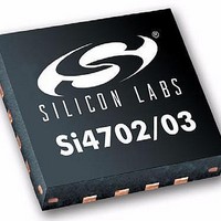
SI4703-B17-EVB Silicon Laboratories Inc, SI4703-B17-EVB Datasheet - Page 13

SI4703-B17-EVB
Manufacturer Part Number
SI4703-B17-EVB
Description
BOARD EVAL SI4703 VERSION B
Manufacturer
Silicon Laboratories Inc
Type
Tunerr
Datasheet
1.SI4703-B17-EVB.pdf
(46 pages)
Specifications of SI4703-B17-EVB
Frequency
76MHz ~ 108MHz
Lead Free Status / RoHS Status
Lead free / RoHS Compliant
For Use With/related Products
Si4703
Lead Free Status / RoHS Status
Lead free / RoHS Compliant, Lead free / RoHS Compliant
Table 8. FM Receiver Characteristics
(V
Parameter
Mono/Stereo Switching Level
Audio Mono S/N
Audio Stereo S/N
Audio THD
De-emphasis Time Constant
Audio Common Mode Voltage
Audio Common Mode Voltage
Audio Output Load Resistance
Audio Output Load Capacitance
Seek/Tune Time
Powerup Time
RSSI Offset
Notes:
D
= V
1. Additional testing information is available in Application Note AN234. Volume = maximum for all tests.
2. Important Note: To ensure proper operation and FM receiver performance, follow the guidelines in “AN231:
3. F
4. MONO = 1, and L = R unless noted otherwise.
5. f = 22.5 kHz.
6. B
7. Typical sensitivity with headphone matching network.
8. Guaranteed by characterization.
9. V
10. |f
11. The channel spacing is selected with the SPACE[1:0] bits. Refer to "6. Register Descriptions" on page 23. Seek/Tune
12. f = 75 kHz.
13. The de-emphasis time constant is selected with the DE bit. Refer to "6. Register Descriptions" on page 23.
14. At LOUT and ROUT pins.
15. Do not enable STC interrupts before the powerup time is complete. If STC interrupts are enabled before the powerup
16. Minimum and maximum at room temperature (25 °C).
A
Si4700/01/02/03 Headphone and Antenna Interface.” Silicon Laboratories will evaluate schematics and layouts for
qualified customers.
timing is guaranteed for 100 and 200 kHz channel spacing.
time is complete, an interrupt will be generated within the powerup interval when the initial default tune operation is
complete. See "AN230: Si4700/01/02/03 Programmer’s Guide" for more information.
= 2.7 to 5.5 V, V
MOD
2
AF
EMF
– f
= 300 Hz to 15 kHz, A-weighted.
3,4,9,12
1
16
= 1 mV.
= 1 kHz, 75
| > 1 MHz,
15
3,4,5,6,9
8,11
3,5,6,8
f
IO
0
µ
= 2 x f
s de-emphasis
= 1.5 to 3.6 V, T
13
3,8,12
14
14
1
8,14
– f
8,14
2
. AGC
Symbol
A
= –20 to 85 °C)
R
C
L
L
is disabled by setting AGCD = 1. Refer to "6. Register Descriptions" on page 23.
1,2
(Continued)
10 dB stereo separation
SPACE[1:0] = 0x, RCLK
(Write ENABLE bit to 1)
tolerance = 200 ppm,
Input levels of 8 and
60 dBµV at RF input
From powerdown
Rev. 1.1
Test Condition
BLNDADJ = 10
BLNDADJ = 10
Single-ended
Single-ended
ENABLE = 1
ENABLE = 0
AHIZEN = 1
(x = 0 or 1)
DE = 0
DE = 1
0.65
Min
55
—
70
45
10
–3
—
—
—
—
—
—
Si4702/03-C19
0.5 x V
Typ
0.1
0.8
34
60
58
75
50
—
—
—
—
—
IO
Max
110
0.5
0.9
80
54
50
60
—
—
—
—
—
3
dBµVEMF
channel
Unit
ms/
k
ms
dB
dB
pF
dB
µs
µs
%
V
V
13


