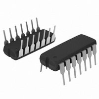
MC1496PG ON Semiconductor, MC1496PG Datasheet - Page 5

MC1496PG
Manufacturer Part Number
MC1496PG
Description
IC MOD/DEMODULTR BALANCED 14DIP
Manufacturer
ON Semiconductor
Specifications of MC1496PG
Function
Modulator/Demodulator
Frequency
300MHz
Rf Type
FM
Package / Case
14-DIP (0.300", 7.62mm)
Maximum Operating Temperature
+ 70 C
Maximum Power Dissipation
33 mW (Typ)
Minimum Operating Temperature
0 C
Modulation Type
Balanced
Mounting Style
Through Hole
Supply Current
0.005 A
Current, Supply
2 mA
Logic Function
Modulator/Demodulator
Package Type
PDIP-14
Temperature, Operating, Range
0 to +70 °C
Voltage, Supply
12 VDC
Supply Voltage Range
30V
Rf Ic Case Style
DIP
No. Of Pins
14
Operating Temperature Range
0°C To +70°C
Digital Ic Case Style
DIP
Ic Function
Balanced Modulator / Demodulator
Rohs Compliant
Yes
Lead Free Status / RoHS Status
Lead free / RoHS Compliant
Other names
MC1496PGOS
Available stocks
Company
Part Number
Manufacturer
Quantity
Price
Part Number:
MC1496PG
Manufacturer:
ON/安森美
Quantity:
20 000
Bias currents flowing into Pins 1, 4, 8 and 10 are transistor
base currents and can normally be neglected if external bias
dividers are designed to carry 1.0 mA or more.
Transadmittance Bandwidth
of the device forward transadmittance as defined by:
of the device forward transadmittance as defined by:
Coupling and Bypass Capacitors
reactance of less than 5.0 W at the carrier frequency.
Output Signal
balanced or single−ended. Figure 11 shows the output levels
of each of the two output sidebands resulting from variations
in both the carrier and modulating signal inputs with a
single−ended output connection.
Signal Input
Modulating
Carrier transadmittance bandwidth is the 3.0 dB bandwidth
Signal transadmittance bandwidth is the 3.0 dB bandwidth
Capacitors C1 and C2 (Figure 5) should be selected for a
The output signal is taken from Pins 6 and 12 either
Carrier
Input
1.0 k
Figure 5. Carrier Rejection and Suppression
g 21S +
V
V
C
S
Figure 7. Bias and Offset Currents
g 21C +
0.1 mF
1.0 k
10 k
C
2
I7
I8
I1
I4
1.0 k
v s (signal)
R1
i o (signal)
50 k
i o (each sideband)
10 k
51
Carrier Null
10
8
1
4
−8.0 Vdc
v s (signal)
51
2
V
0.1 mF
EE
R
MC1496
⎥
e
14
C1
I10
= 1.0 k
V c + 0.5 Vdc, V o + 0
51
10
5
6.8 k
3
8
1
4
−8.0 Vdc
6
12
1.0 k
2
V
⎥
MC1496
EE
14
V
I6
I9
12 Vdc
V o + 0
I10
1.0 k
−
R
V
e
CC
I5
2.0 k
3
5
6.8 k
3.9 k
12
R
6
L
12 Vdc
http://onsemi.com
TEST CIRCUITS
V
I9
CC
I6
3.9 k
R
+V
Signal Input
L
−V
Modulating
Carrier
5
o
o
Input
Negative Supply
series with V
current sources.
Signal Port Stability
oscillation may occur. In this event, an RC suppression
network should be connected directly to each input using
short leads. This will reduce the Q of the source−tuned
circuits that cause the oscillation.
insert a 1.0 kW resistor in series with the input (Pins 1, 4). In
this case input current drift may cause serious degradation
of carrier suppression.
V
V
C
S
V
Under certain values of driving source impedance,
An alternate method for low−frequency applications is to
0.1 mF
EE
10 k
NOTE: Shielding of input and output leads may be needed
Figure 8. Transconductance Bandwidth
should be dc only. The insertion of an RF choke in
Z
(Pins 1 and 4)
Signal Input
in
1.0 k
Figure 6. Input−Output Impedance
50 k
51
10 k
Carrier Null
to properly perform these tests.
0.5 V
EE
+
can enhance the stability of the internal
0.1 mF
−
51
10
8
1
4
−8.0 Vdc
2
51
MC1496
R
10
8
1
4
14
e
−8.0 Vdc
= 1.0 k
2
1.0 k
V
EE
MC1496
14
V
510
−
1.0 k
R
6.8 k
3
5
e
6
12
3
5
6.8 k
12
6
50 50
Z
2.0 k
10 pF
+V
out
−V
V
12 Vdc
CC
o
o
+V
−V
0.01
mF
o
o


